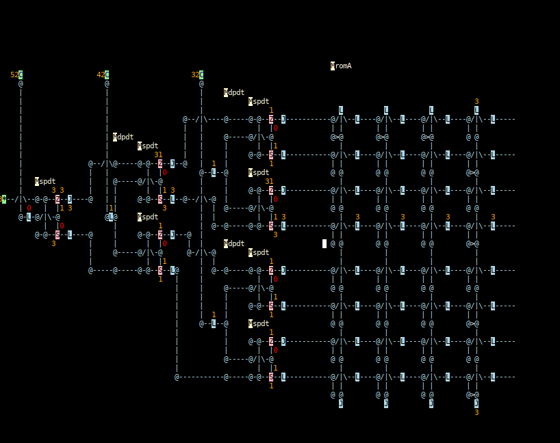
OK so the hardware lacks a schematic. So I have started coding a logic simulator in Golang for this project which runs in ordinary terminals (it's a T.U.I) This first simulation is also the first schematic.
You can see a recording of the simulator here:
The Betula simulation of the decode and state transition ROM
Here's a snapshot:

There are three address lines which are decode by the 7 relay encoder on the left. The eight select lines are connected to an array of diodes on the right which are going to make up the program read-only-memory of the Wolffia computer.
Discussions
Become a Hackaday.io Member
Create an account to leave a comment. Already have an account? Log In.