(Mandatory "I'm not dead just busy" comment)
I've got exciting views for you: I've gotten to the point where I can exchange data with the phone, reversed the init sequence, and now have a phone that is almost fully functional (as in, I can make calls with coins or cards); I also figured out how the phone talks with the card reader, and I can read the cards' contents through said reader.
However, as you can see, the info here on Hackaday is waay behind the actual progress. I'm now in the process of at least writing some kinda-complete documentation, even if this means I'm probably gloss over some details about how I got to this info. That said, the first thing I'm gonna concentrate on is the "mistery" SCL1054-V4 custom chip.
What does this thing do, anyway?
Long story short, it has three functions:
- RAM expansion: it fills the gap between addresses 0x0140-0x1FF with extra RAM; not all of this is used by the code, but it's there.
- Extra I/O ports: it adds 4 memory mapped ports, one of which is bidirectional (the other two are outputs only).
- Address decoding logic: all logic needed to map said RAM and ports, plus the ROM, in memory is handled internally.
In more detail:
1) The RAM
Not much to say here. It's 192 bytes of extra RAM, mapped 0x0140-0x1FF, which are directly accessible by the phone's microcontroller.
2) The ports
There's three 8 bit ports + a 1-bit one, controlled via 5 registers:
- SCL_DATA, bidirectional; data register is mapped to 0x0021, direction register is 0x0022 (bits that are set means the corresponding line is an output). This is used to drive the "data" bus to which the various buffers on the digital board are attached to.
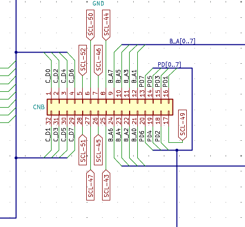
- SCL_ADDR, output only; data register is 0x0020. This drives, through latches U5 and U6, the address+control buses for the external RAM+ROM daughterboard. Note that bits 7, 6, 5, 3 are also used to control the LCD reset signal + the three solenoid drivers. Check schematics for more details
- SCL_CTRL, output only; data register is 0x0021. This is used for miscellaneous outputs; again, check schematics for more details, but the lines from this port are used both to direct I/O to and from the data bus, to manage the serial communications to the card reader and to control the main motor. On the schematics, this port's pins are marked with SCL-nn where nn is the number of the corresponding pin on the SCL's package; SCL-43 corresponds to bit 0 and so on.
- SCL_BANK, 1-bit only; data register is 0x0024 (only bit 0 is used) and it's used to select the ROM bank (drives A14 on the ROM). This was an especially important discovery because the ROM code now makes a lot more sense.
3) Miscellaneous combinatorial logic
All the logic for mapping ports+RAM+ROM in memory is integrated in the SCL chip.
Discussions
Become a Hackaday.io Member
Create an account to leave a comment. Already have an account? Log In.