 f4hdk
f4hdk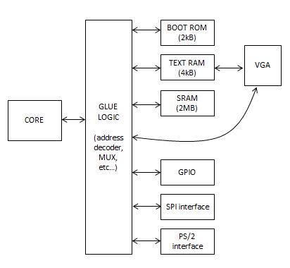
The CPU is a “Von Neumann” one (as opposed to Harvard), for simplicity. There is only one external bus (data + address), for all memory and peripherals.
The 16bits words are organized as “little endian”, because I think that it is logic.
Frequency:
The biggest frustration of this project is the frequency. Theoretically, the CPU could have run at 50MHz. At this frequency, 3/4 of the time is dedicated to the CPU for computing, and 1/4 of the time is dedicated to the VGA. Therefore, the CPU is equivalent to 37MHz.
But I had lots of difficulties to understand FPGA timing constraints. I am 100% autodidact, and this my first FPGA project. The FPGA was not reliable at 50MHz, and I was stuck 2 months trying to solve this problem.
I wanted to go on with other parts of the project, and not remain stuck. That’s why I decided to reduce drastically the frequency to 25MHz. At this frequency, 1/2 of the time is for the CPU, and 1/2 for the VGA. This is equivalent to 12Mhz, and global performances are divided by 3.
This is a big disappointment.
8bits – 16bits:
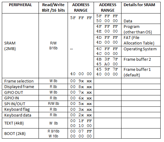
Warning, data can be manipulated with 8 bits or 16 bits.
But among all the peripherals mapped to the address plan, only the SRAM can be accessed via 8 or 16 bits.
The boot Rom (in reality this is a RAM) can only be accessed with 16bits.
The text RAM only accepts 8bits access, and can only be written by the CPU, not read.
The SPI is 8 bits only.
There is no protection in the compiler, and it is easy to make errors.
Discussions
Become a Hackaday.io Member
Create an account to leave a comment. Already have an account? Log In.