So 5 weeks ago I rediscovered this GPstar Plus 365 while having a clearout, and decided to power it up and hopefully (finally, 10+ years down the track) put it to use.
So I put it on the bench, power cable and antenna connected, hit the power, and.... nothing.
Not to be discouraged after a couple of goes I disassembled the enclosure for a closer look.
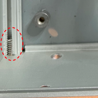
The casing itself is interesting - there are four machine screws at each end, if you undo one end then the side slides out sideways. In fact if you are not careful all the panels slide out and you have things falling everywhere... kind of ingenious and fiddly at the same time. You can see the thread cavities as the are 1/4 open, where you slide in the panels...

Anyway with voltmeter in tow it didn't take long to discover the PSU had no output.

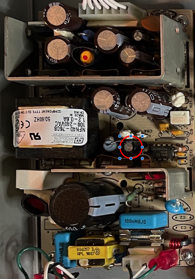
Circled is the capacitor I eventually worked out had failed.
To the left of that is a resistor which has over 300VDC across it. Given this was an open mains switch mode power supply I was already suspicious, so making sure I used a meter on 1000V mode with one hand in my pocket and well insulated leads when probing...
To the right of the circled capacitor is the control chip, a UC3842AN. It turns out this was a widely used part at the time.
To cut a long story short, it didn't take too much googling to discover that there seem to be a number of forums or blogs in Eastern Europe for some reason where people have fun reverse engineering and discussing such power supplies, and along with the data sheet and a couple of hours tracing the circuit I worked out this design was fairly close to that provided as a reference by the manufacturer.
Across the week I traced out enough of the circuit to understand how it worked.
One interesting thing is that the control chip won't actually start working as a frequency controller for the SMPS until the input voltage for it reaches around some DC voltage (I think in the order of 15, I don't have the data sheet open while writing this), in this case it was only coming up to about 8. To a very very rough approximation of reality* this is to do with ensuring the chip can properly drive the FET and the main transformer: to bootstrap power on, there is a capacitor which first charges up past that voltage and then feeds the chip with a zener regulator, this is in parallel with the actual voltage generated through a rectifier on a secondary tap of the transformer once things are up and running, also clamped by same Zener. However that secondary tap is not running at power on, and when the capacitor fails, it won't provide the necessary bootstrap voltage, and the chip won't start switching the FET. This can be confusing when first drawing up the circuit.
This all happens in the section in the middle between the two heatsinks - the upper in particular marks an isolation boundary between mains-hot and the output stage, provided by the transformer, and also an optocoupler providing feedback.
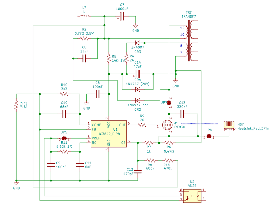
I redrew my sketch in Kicad to make it easier to read.
(Picture -

There you go, the zener CR4 is clamping the bootstrap Vcc to 20V.
The voltage between L? and R5 is full rectified mains, so watch out!
The failed capacitor was C14, 47 uF.
The 14 ohm resistor was looking decidedly brown from heat, I guess it is to limit inrush to charging the capacitor and when it is failed the voltage drop and power is larger.
A week later, when I desoldered C14 (more about that in a later post) it gave me an excuse to finally buy an ESR meter with which I confirmed that it was indeed failed, with a very high internal resistance and low capacitance.
(*I do understand all the math and circuit theory, I'm just not spending the bandwidth documenting it, but by all means feel free to post in the comments for the benefit of other readers :-) :-) )
 pastcompute
Discussions
Become a Hackaday.io Member
Create an account to leave a comment. Already have an account? Log In.