 Christoph Tack
As a power bank, this device should be able to supply 5V/1.5A, because that's what each of my tablet and phone are drawing during charging.
Dedicated power bank ICs exist that incorporate a boost converter and battery charging and protection circuitry (Thinkplus MP5043/MP5045, Hotchip HT4936S & PB0059E, Injoinic IP5306). These don't need many external components. The main drawbacks are their limited output current capability and they turn off when the output current is too low.
Another option is to design our own PCB using DC/DC-converters available : FeelingTechnology FP6276, FP6293, FP6298 or XYSemi XR2981. Designing our own power supply board would take more time.
Option 1: 5V/3A boost converter
AliExpress 5V 3A DC-DC Step Up Power Module : €1.03/pce
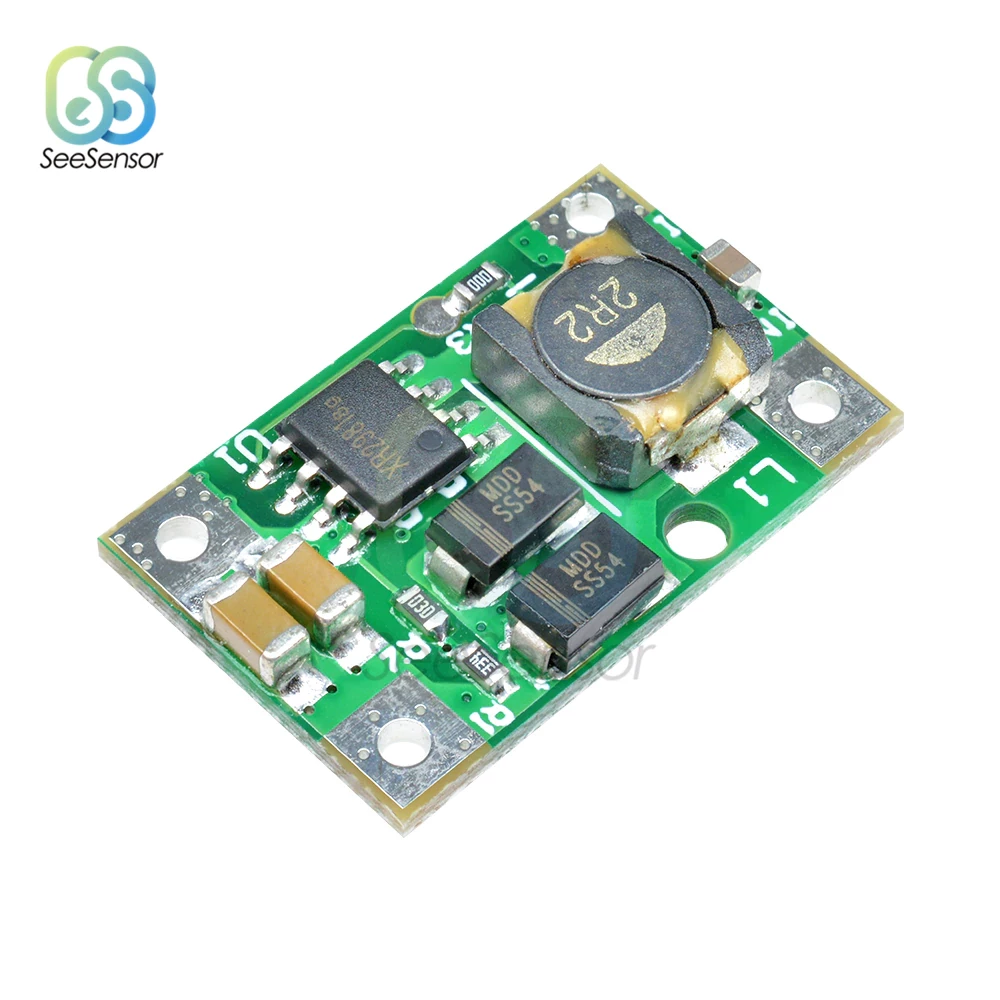
Uses Xysemi XR2981 boost converter., can also be found as H&Msemi HM9228B (hmsemi.com)
- A TPS2514 will be needed on the USB-data lines to tempt the devices into drawing 1.5A instead of the normal 500mA.
- Tablet : with tps2514 : 1.35A, without : 0.476A
- smartphone (after a few seconds) : with tps2514 : 1.18A, without : 0.457A
- The no-load input current is 150µA (at Vin=3.7V).
- There seems to be very little filter capacitance on this board. Ripple will likely be quite high.
- The schottky diode has a Vf of 335mV at 1A and 359mV at 2A.
- Inductor Rdc = 11mΩ
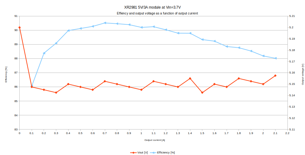
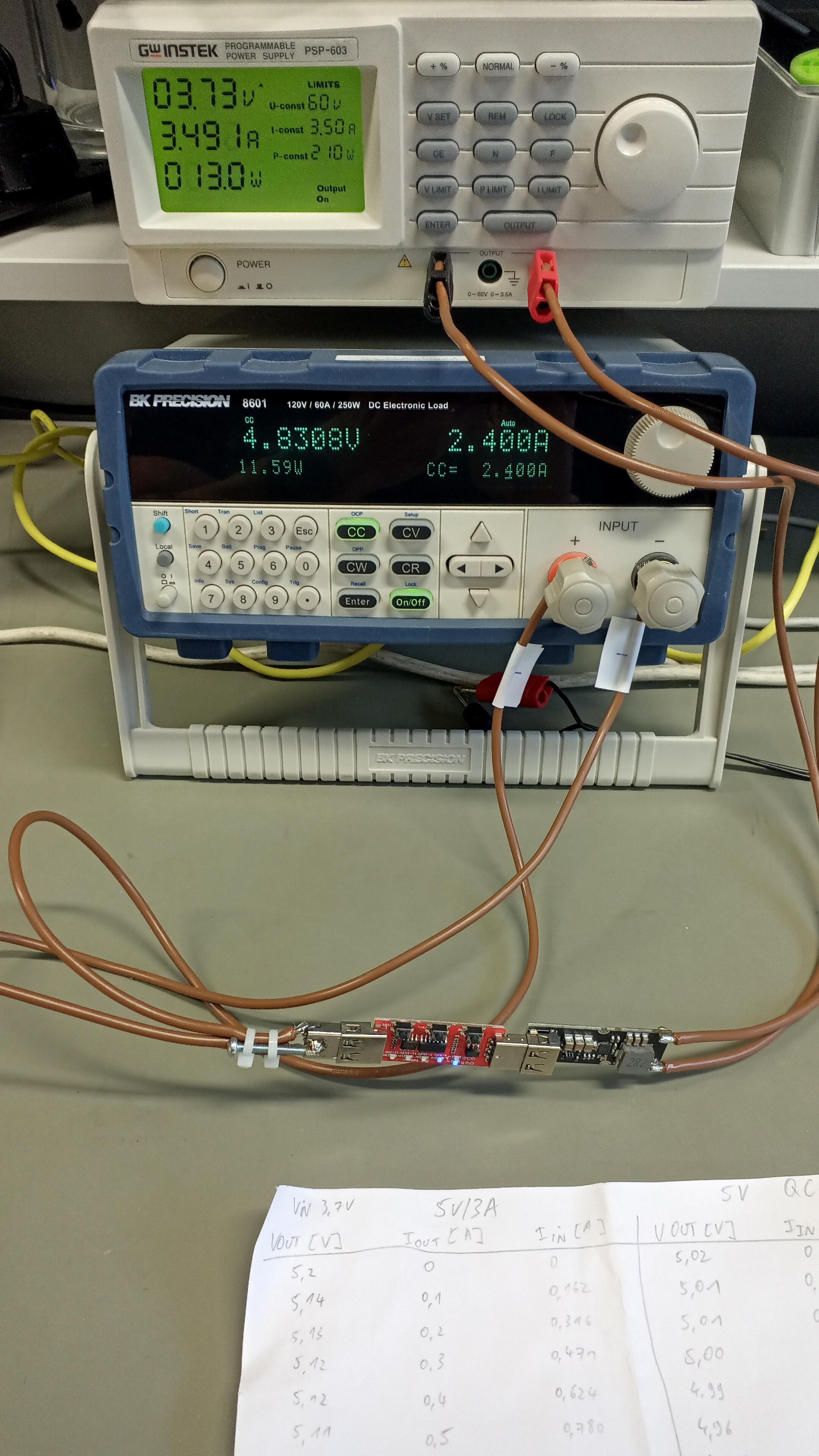
The measurement stopped at an input current of 3.5A, which was the maximum for my lab power supply.
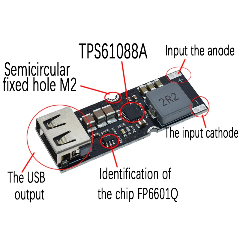
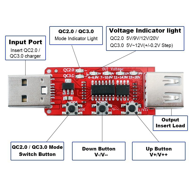
Option 2 : Qualcomm QC2.0/3.0 Fast charge module TPS61088A
AliExpress TPS61088 Boost power module : €2.21/pce
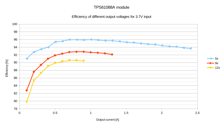
This module is more expensive, but it has the potential of faster charging by boosting the USB-voltage to 12V:
- 5V/3A : a Blackview cellphone and Samsung Galaxy tablet settle for this mode, drawing 5V/1A.
- 6.2V (=QC3.0) : used by cellphone BQ Aquaris X Pro
- 9V/2A
- 12V/2A
The no-load current is 548µA with a supply voltage of 3.7V. The EN-pin of the TP61088 is hard connected to VCC. Even disabling the TPS61088 would still leave us the 200µA current draw of the FP6601Q.
UVLO falling is 2.4V after which 0.5A is drawn. If the input voltage rises again above 2.6V, normal operation is resumed.
The TPS61088 is a synchronous boost converter, which minimizes losses that would otherwise be caused by the schottky diode. There's also a larger inductor used here, which probably has a lower Rdc than the one in the 5V/3A-module.
The measured efficiency matches the TPS61088A datasheet very well.
To be able to test it with an electronic load, I ordered a QC2.0/QC3.0 tester (AliExpress QC2.0 tester : €3.53/pce).
A better USB tester is the Fnirsi FNB38.
Another option is the Lithium Battery Charging and Discharging TYPE-C Integrated Board PD Bidirectional 18W Fast Charging Mobile Power Supply Bank. It uses an unknown IC. Idle current is unknown as well. Support for QC3.0 and USB-PD 3.0.
Discussions
Become a Hackaday.io Member
Create an account to leave a comment. Already have an account? Log In.