 Christoph Tack
Driver for main light source
The selected light source is a 12V LED-COB panel. There are not many circuit options to consider here. A boost converter will do the job just fine. In the current component shortage situation, we'll have to look for a solution that allows for multiple second source components.
That brings us to the following:
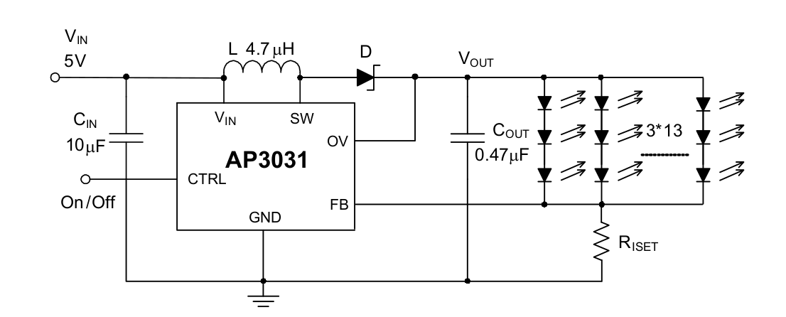
Pin list :
- SW : Switch
- AP3031 : 1MHz, max. 1.4A
- RT4533 : 1.1MHz, max. 1.2A
- FAN5333A : 1.5MHz, max. 1.5A
- MP302DJ : 1.3MHz, max. 1.3A
- MIC2291 : 1.2MHz, max. 1.2A
- GND
- FB : feedback voltage :
- AP3031 : 200mV
- RT4533: 200mV, RT4533A=300mV
- FAN5333A: 110mV
- MP3202 : 104mV
- MIC2291 : 95mV
- CTRL : enable pin: high = ON
- OV : over voltage protection
- AP3031 : max. 17.5V
- RT4533=36V
- FAN5333A, no over voltage protection, only 15% over current protection
- MP3202 : 28V
- MIC2291Y : not present
- VIN : input voltage
- AP3031 : 2.7V→16V
- RT4533: 2.5V→5.5V
- FAN5333A: 1.8V→5.5V
- MP3202DJ: 2.5V→6.0V
- MIC2291 : 2.5V→10V
Sources :
AP3031KTR-G1 has a 50µA quiescent current (CTRL=0V), so an external FET will be needed.
- RT4533GJ6 : 300nA quiescent current (EN=0V). Sold out Digikey end of 2021.
- FAN5333ASX: 100nA quiescent current (/SHDN=0V), but 1µA switch leakage? (2023: obsolete)
- MP3202DJ : 100nA quiescent current (VEN=0V)
- MIC2291Y : 100nA (VEN=0V)
Driver for secondary LEDs
The UV-LED has a forward voltage of up to 3.8V, while the Li-Ion battery is only 3.6V.
Reusing primary LED driver
We can cut costs by reusing the LED-driver for the main LED-string. The sense voltage is 200mV for the AP3031, which is quite a low voltage. This enables us to use NMOS-FETs to switch the LED-strings without need for gate bootstrapping.
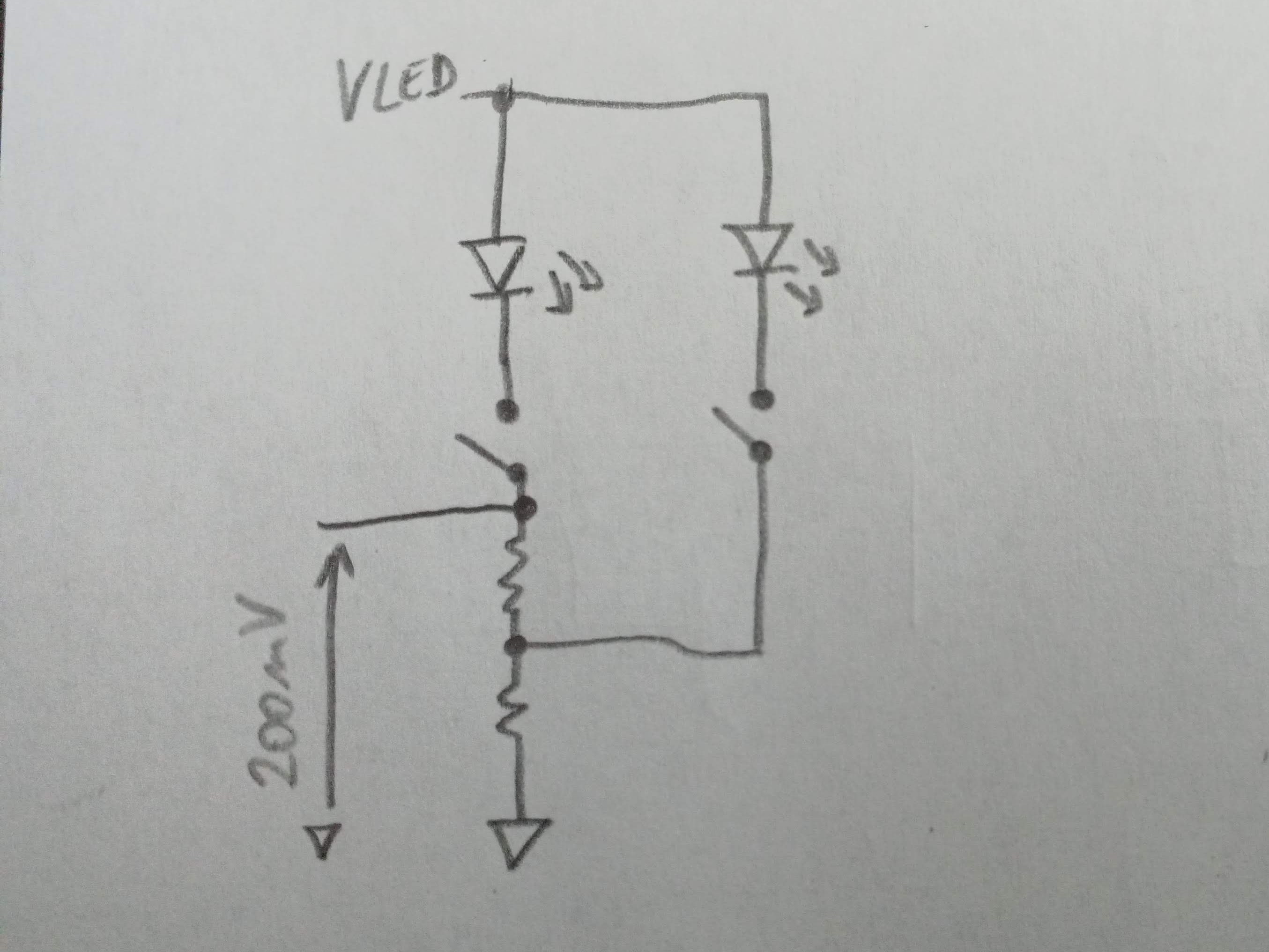
By the arrangement of the sense resistors as shown in the picture, we can make each LED string work with a different LED-current.
Design consideration : Linear LED driver
We need a sense resistor in series with the LED. This causes an extra voltage drop, which requires a higher supply voltage. The 5V booster could be used to provide power for the linear LED driver. It's there already anyway.
The problem with this approach is the rather limited efficiency, both of the 5V booster for such low currents and of the nature of the linear LED driver itself.
An LMV321A opamp-current source with an FDV301 drive transistor and with 100mV over the sense resistor doesn't allow for the full 30mA output of the LED. At least 3.4V is needed. To be able to dim it, independent of the supply voltage, an extra voltage reference is needed. This is becoming a bulky circuit.
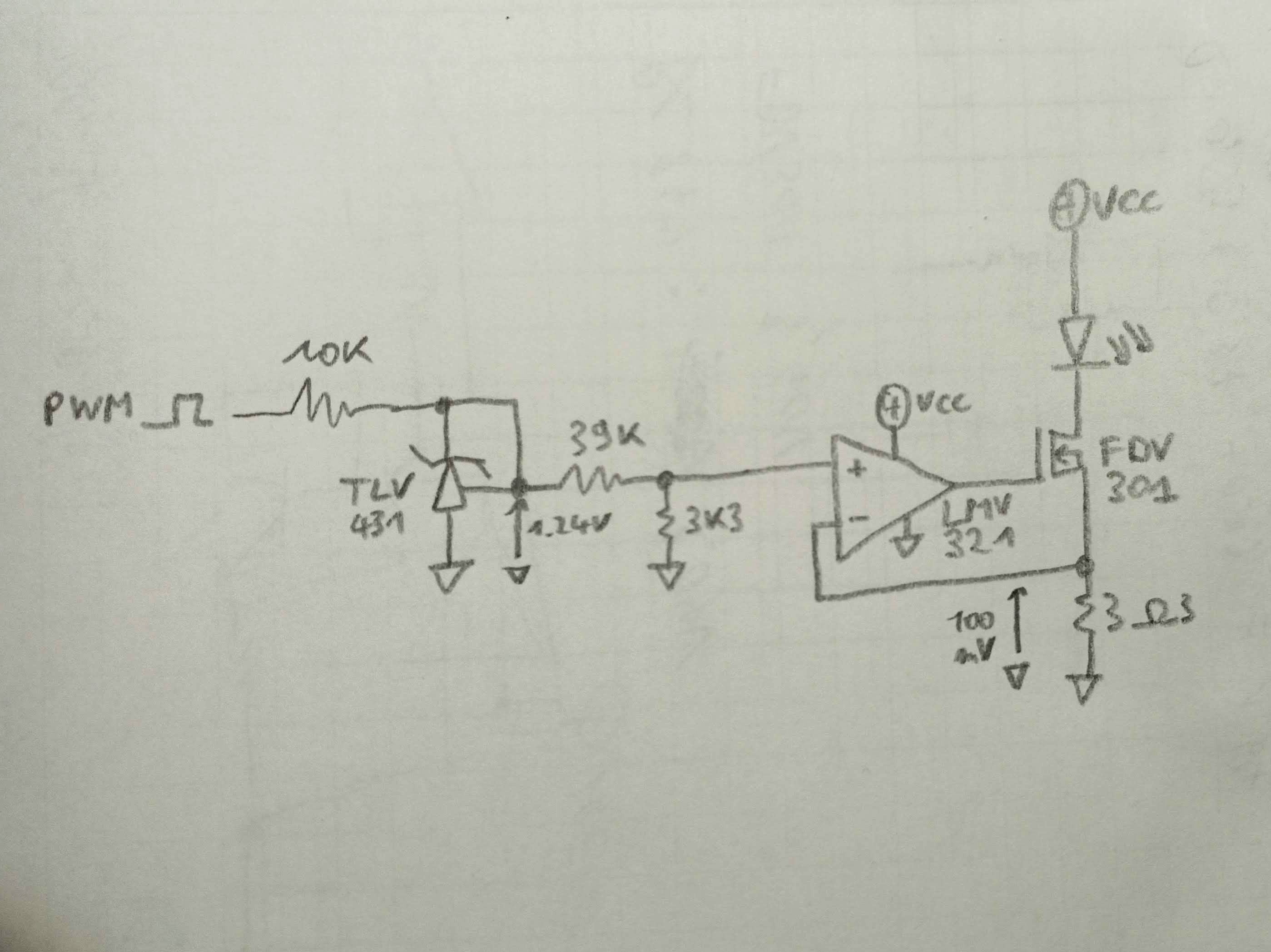
The AP2502 could be used instead, but unfortunately it's a single source component.
As it turns out, this circuit will cost more (both in money and PCB-area) than using the AP3031 with two UV-LEDs.
Design consideration :Switching LED driver
See #TritiLED for more info.
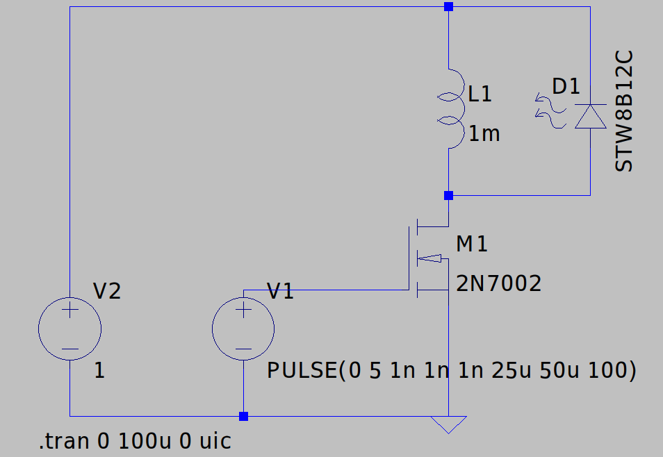
This is the basic circuit of the switchable LED driver. NMOS-transistor M1 conducts, causing the current through L1 to rise. When M1 stops conducting, L1 will dump its magnetic energy inside the (blow-back) LED D1.
A trade-off has to be made between the switching frequency and the inductor value. Smaller inductors are cheaper but require higher switching frequencies, which the MCU might not be able to deliver.
This circuit has limited dimming range. The pwm-resolution is 0.125µs. The maximum ON-time is around 12.5µs (50mA peak, 4V power supply, 1mH inductor). Which means we have a dimming ratio of only 1:100.
The ON-time regulation is very tricky in this circuit. If the ON-time is too long (software bug or glitch), we'll end up blowing up the mosfet and the inductor.
As a result this circuit will only be used when the NMOS is controlled with a fixed duty cycle.
Design consideration :Switching LED driver with selectable LED-output
The design will feature several LEDs, but we don't want a separate driver for each LED. That would add too much cost and PCB space. Using the following circuit, V3 selects whether to light D1 or D2. When M3 conducts, D1 will be lit. When M3 is off, D2 provides a blow-back path for the energy in L1. This only requires one extra NMOS-transistor. Several D1/M3 stages could be added in parallel to D1/M3 to allow for more selections.
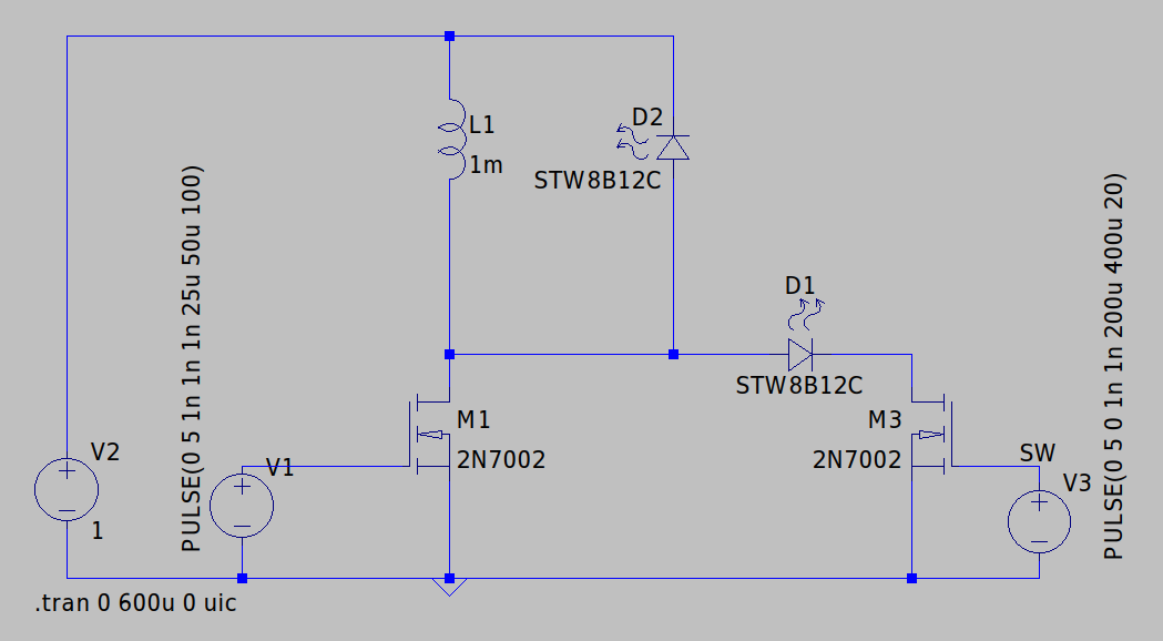
The problem with this last circuit is that it no longer works when the supply voltage is higher than the LED forward voltage. If M3 is ON, then D1 would be conducting, even in the idle state (when M1 is off for a long period of time).
Discussions
Become a Hackaday.io Member
Create an account to leave a comment. Already have an account? Log In.