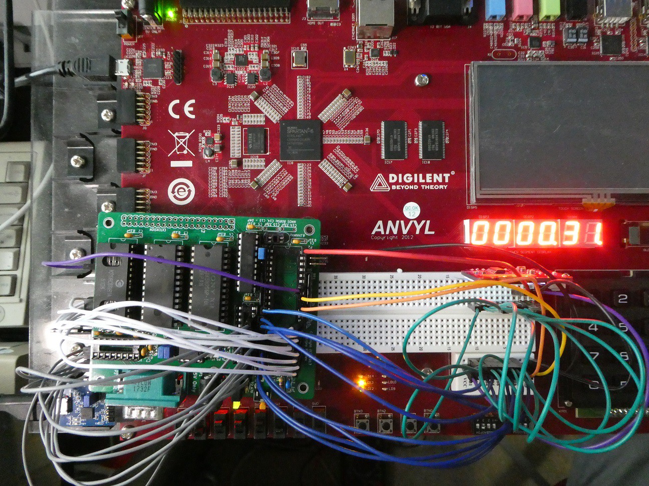
For this project I used a cool little 8085-based single board computer (8085 Minimax) described and graciously provided to me by Ken Yap (thanks again!). I was actually in the process of soldering together the board, and decided to use a verification step before plugging in my vintage Soviet CPU to see if there will even be a chance for it working or not...
The hardware setup is simple but a bit messy affair:

Few notes:
- 8085 IO/M signal (purple wire) is simply switchable to IO (high) to M(emory) (low) using a micro-DIP on the FPGA board. The HEX I/O has no idea about it, it just sees IO space as another 64k address map space (of course with 256 repetitions because typically in 8080-family systems upper 8 address lines are not decoded (Z80 introduced 16-bit IO to some degree, and then HD64180 has a full 64k IO address map)
- 8085 has multiplexed lower address A7..A0 with data bus D7..D0, giving AD7..AD0 bus. Typically a 8-bit latch (like 74x573) enabled by ALE captures the low address early in memory access cycle. To simplify, I left this IC unpopulated on the board and connected the low memory address wires (gray) directly to its output socket pins.
- Minimax 8085 of course takes +5V DC - I am sourcing its modest consumption (esp. because the power hungry NMOS CPU is not there!) with a 3.3V to 5V step-up regulator.
- Connecting nominal 3.3V (FPGA) to nominal 5.0V (SBC) is a "circuit crime". But I could get away with it in this case as the modern RAM / ROM used has max "0" voltage and min "1" voltage signals that are within margins.
- 4 additional PMOD signals are used for UART - this is how the Intel HEX files are uploaded/download during runtime.
This is how these connections look in VHDL (top file of the project):
                --PMOD interface
                JA1: inout std_logic;    -- Connected to USB2UART
                JA2: inout std_logic;    -- Connected to USB2UART
                JA3: inout std_logic;    -- Connected to USB2UART
                JA4: inout std_logic;    -- Connected to USB2UART
                JB1: out std_logic;    -- GRAY 74F573.19 A0
                JB2: out std_logic;    -- GRAY 74F573.18 A1
                JB3: out std_logic;    -- GRAY 74F573.17 A2
                JB4: out std_logic;    -- GRAY 74F573.16 A3
                JB7: out std_logic;    -- GRAY 74F573.15 A4
                JB8: out std_logic;    -- GRAY 74F573.14 A5
                JB9: out std_logic;    -- GRAY 74F573.13 A6
                JB10: out std_logic;    -- GRAY 74F573.12 A7
                JC1: out std_logic;    -- WHITE 8085.21    A8
                JC2: out std_logic;    -- WHITE 8085.22    A9
                JC3: out std_logic;    -- WHITE 8085.23    A10
                JC4: out std_logic;    -- WHITE 8085.24    A11
                JC7: out std_logic;    -- WHITE 8085.25    A12
                JC8: out std_logic;    -- WHITE 8085.26    A13
                JC9: out std_logic;    -- WHITE 8085.27    A14
                JC10: out std_logic;    -- WHITE 8085.28    A15
                JD1: out std_logic;    -- PURPLE 8085.30 IO/M (low for memory access)
                -- breadboard signal connections
                BB1: inout std_logic;    -- BLUE 8085.12 AD0
                BB2: inout std_logic;    -- BLUE 8085.13 AD1
                BB3: inout std_logic;    -- BLUE 8085.14 AD2
                BB4: inout std_logic;    -- BLUE 8085.15 AD3
                BB5: inout std_logic;    -- BLUE 8085.16 AD4
                BB6: inout std_logic;    -- BLUE 8085.17 AD5
                BB7: inout std_logic;    -- BLUE 8085.18 AD6
                BB8: inout std_logic;    -- BLUE 8085.19 AD7
                BB9: out std_logic;        -- ORANGE    8085.31 nWR
                BB10: out std_logic;        -- YELLOW    8085.32 nRD
 zpekic
Discussions
Become a Hackaday.io Member
Create an account to leave a comment. Already have an account? Log In.