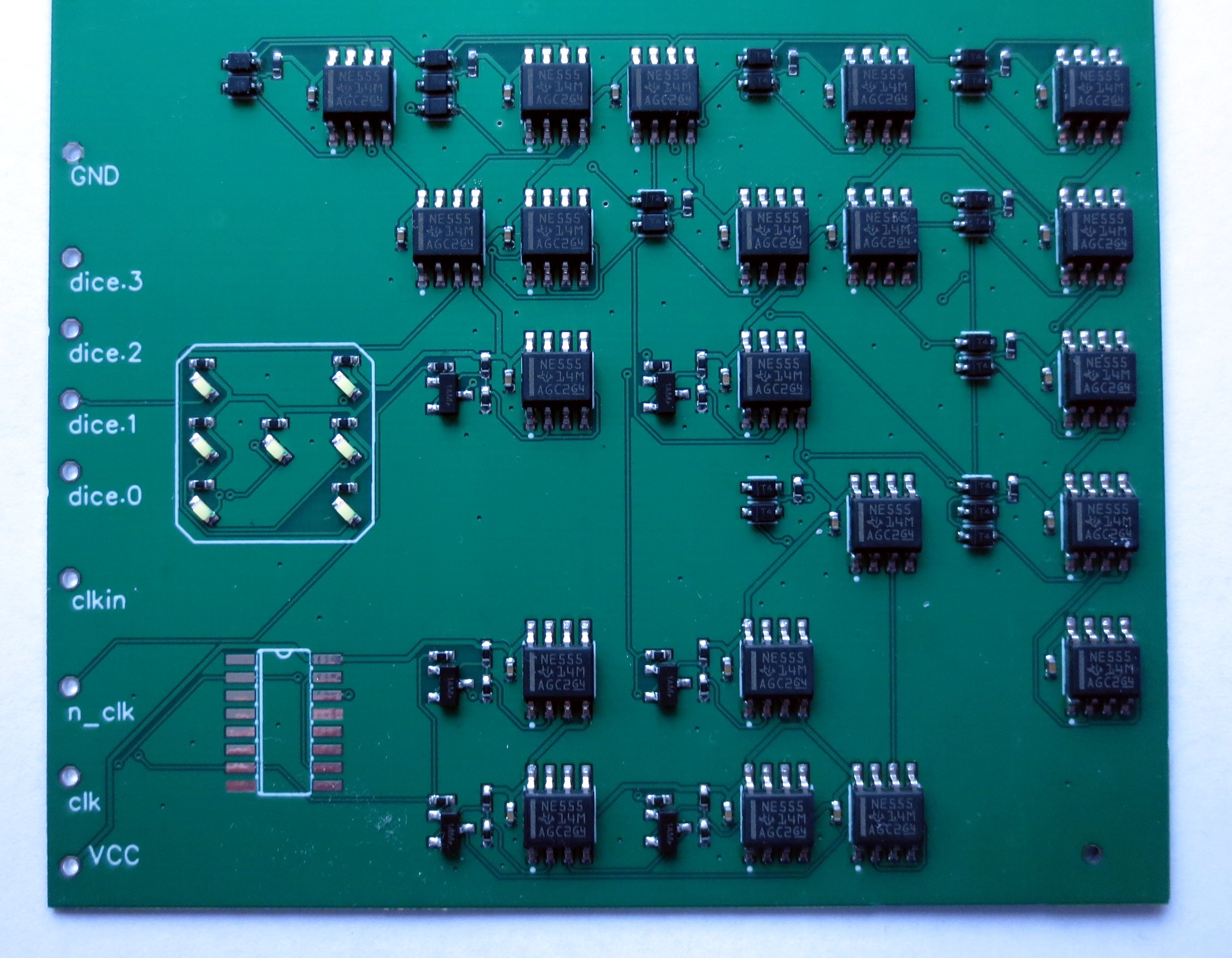
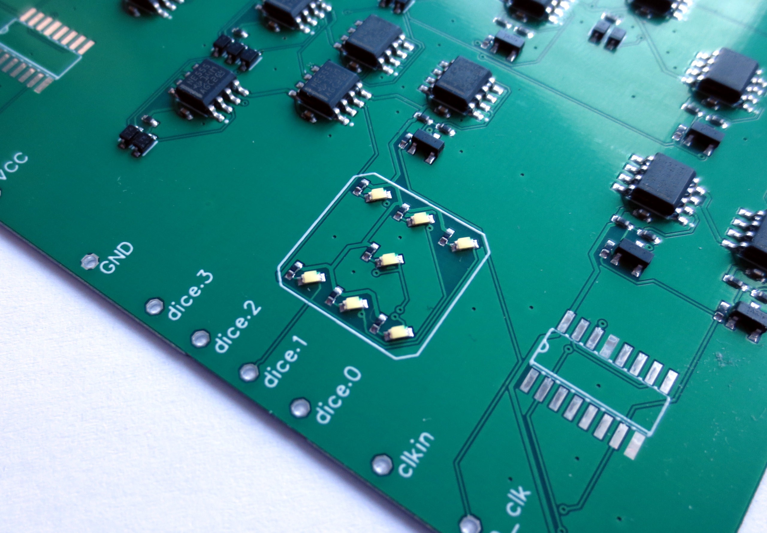
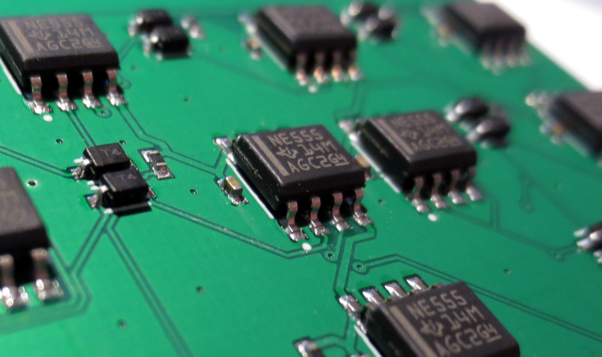
The PCB in all its glory
Validation
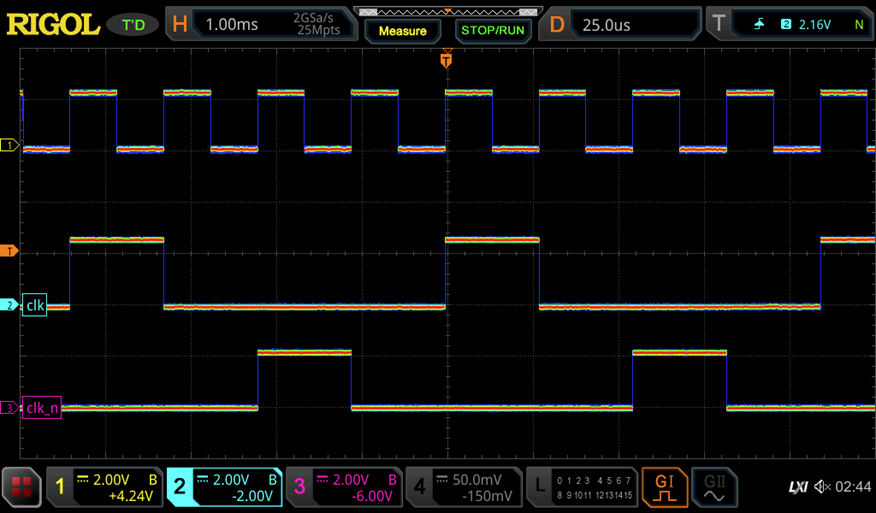
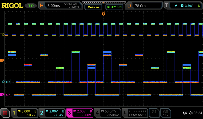
First step is to test the clock generation. The scope image below shows how the CD4017 generates the nonoverlapping two phase clock (clk and clk_n) from the input clock signal. It appears that the CD4017 is able to operate only up to ~1.3 MHz, so maximum generated output clock is around 300 kHz. This is not a big issue since this is still far beyond the capabilities of NE555 logic.
 Unfortunately, things did not go as smoothly from there. After some debugging I found that I had to raise the operating voltage to 6V for the dice to function properly. The reason for that is the loading of the clock nets when the input to the latches is low. In that case, the output of the CD4017 has to drive a VBE-diode and a 3.3kohm resistor vs ground. Apparently this is too much and we can observe a significant drop in output voltage which which does not allow the NE555 flip flop to switch. (See here for the latch design)
This is apparant in the scope image below where the high level of the clock signal varies depending on state of the dice.
Apart from raising the voltage, another fix would be to increase the base resistor value of the pass-gate devices in the latch or introducing some NE555 as clock drivers. Of course, a much cleaner way would be to construct latches from diodes and NE555 like mike has done in his project. But this would raise the number of NE555 further.
Dice action!
All said and done, see below for a short clip of the dice operating in NE555 logic!
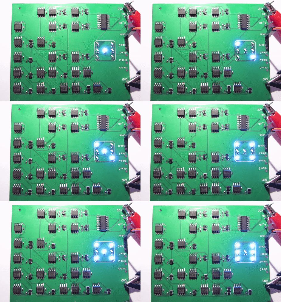
And another logic type proven in practice! Would I use it for other designs? Probably not. The area consumption is huge, cost is quite high, power consumption is higher than even RTL (~70 mA for the dice) and it is by far the slowest logic type I ever investigated.
Unfortunately the version I built based on ANDN2 gates does not seem to work properly. Some more debugging is needed to figure out the root cause.
 Tim
Tim
Discussions
Become a Hackaday.io Member
Create an account to leave a comment. Already have an account? Log In.