MKHBC-8-R2 - Multipurpose 8-bit Homebrew Microcomputer. Design and Specifications.
1. Architecture of the system.
The system is intended as a hobbyist computing/microcontroller expandable platform. The CPU of choice is MOS 6502 compatible microprocessor. The design is a passive back-plane multiboard computer. It will consist of 2 buses:
- 3-slot CPU bus for CPU, RAM and graphics cards.
- Buffered 4-slot I/O expansion bus for other peripherals.
Other features:
- Programmable 8-input prioritized interrupt controller.
- Optional Real Time Clock with non-volatile battery backed SRAM for BIOS settings (DS1685).
- Optional banked RAM (128 kB: 16 kB x 8).
- Built in I/O port (6521/6821 PIA or 6522 VIA) for interfacing peripherals (joystick, I2C, SPI, serial keyboard, digital I/O).
- Control panel with built in reset key, NMI reset key, power switch and (connected to built in VIA I/O port): 16x2 LCD (or better) display, buzzer and 2 programmable keys.
1.1. Memory Map.
$0000 - $7FFF: Base RAM, 32 kB.
$6000 - $7FFF: Optional Video RAM, 8 kB.
$8000 - $BFFF: Banked RAM, 16 kB space x 8 banks = 128 kB.
$C000 - $C7FF: I/O space, 8 slots x 256 Bytes = 2 kB.
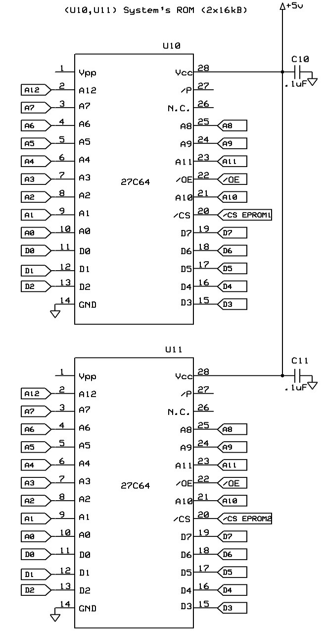
$C800 - $FFFF: EPROM, 14 kB.
2. Back plane/motherboard.
Motherboard will consist of CPU bus with 3 64-pin slots for primary components of the computer system.
The primary components will include:
- CPU card with EPROM, base RAM, reset/IRQ/NMI circuits and I/O address decoding circuits.
- Optional RAM expansion card.
- Optional RTC and battery backed SRAM card.
- Optional graphics controller card.
The I/O address decoding circuit will decode 8 I/O address spaces, from which 4 (slots 0-3) will be used for internal system's built-in I/O devices (RTC, memory bank switch register, interrupt controller, VIA I/O port) and the rest of the slots (4-7) will be used in expansion bus.
Planned allocation for internal I/O slots in mother-board mode of operation:
- Slot 0: RAM bank switching register.
- Slot 1: RTC and non-volatile (battery backed) SRAM for BIOS settings (DS1685). The RTC circuit with backup battery will be assembled on the same CPU-bus card as banked RAM.
- Slot 2: Prioritized Interrupt Controller. The circuit will be integrated on the motherboard, its control registers connected to the I/O bus.
- Slot 3: I/O. 6521 (MC6821) PIA or 6522 VIA compatible I/O chip. The I/O pins would be buffered and exported to the 40-pin connector. Using this connector, external devices could be connected to the system. E.g.: general purpose control panel (keypad, LCD, LED-s, joystick ports, I2C,/CAN/SPI ports etc.).
Planned allocation for internal I/O slots in SBC mode of operation:
- Slot 1: UART/RS-232.
- Slot 3: I/O (PIA or VIA).
Motherboard will also consist of fully buffered 4-slot 40-pin I/O expansion bus, which is intended for expansion cards designed by user. That bus will use I/O slots 4 through 7. The bus will allow to address 256 registers in each slot (8 address lines), will have full data bus and all CPU signals as well as derived from CPU supporting signals (/OE, /WE). Each expansion card can be a source of IRQ interrupt signal.
Planned I/O expansion cards (for slots 4-7):
- Mass storage controller (SD, flash, IDE).
- SID (Commodore) based sound card.
- UART/RS-232 (MC6850). - built
Planned CPU bus expansion cards:
- Banked memory 128 kB + battery backed RTC and non-volatile SRAM. - built
- Video Adapter (MC6847 VDG - Video Display Generator, but also considering more contemporary PICASO board, VGA controller with serial port as command input/output).
User input:
User input interface will be realized with full alphanumeric keyboard and digital joystick (C64, Nintendo, Atari compatible). The keyboard may be serial (UART, I2C) or classic matrix to be scanned in periodic interrupts generated by RTC chip DS1685 or timer in VIA adapter. If keyboard is to be serial, it must be the source of the IRQ interrupt which will read and store the input in software buffer, unlike matrix keyboard which is a passive device and must be scanned periodically in timer based interrupt, its input stored in software buffer.
3. CPU card.
CPU card design is a compromise between two modes: the SBC mode (will be able to function outside the motherboard with some circuitry attached to its bus and i/o connectors) and also will be able to work in parallel bus back plane based expandable system.
CPU card components:
- Rockwell 6502 microprocessor.
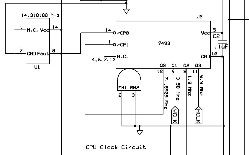
- CPU clock circuit.
- CPU reset circuit.
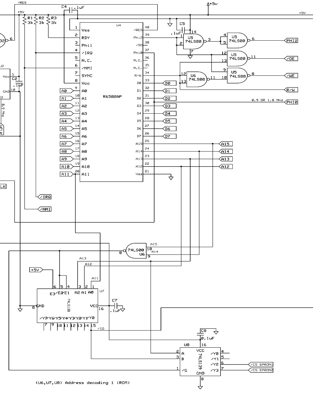
- EPROM, base RAM and I/O address decoding.
- EPROM firmware memory and base 32kB RAM memory.
- 6850 UART / RS-232 controller. (this circuit will not be physically built on the CPU board but will be built on a separate board and connected via 40-pin I/O connector).
- 64-pin male connector compatible with CPU bus slot on the motherboard.
- 40-pin IDE connector with the same pinout like expansion bus – this connector will serve the purpose in SBC mode.
CPU card together with UART card connected via 40-pin IDE style connector and mini-mobo board connected via 64-pin euro-socket connector will be able to work standalone like SBC board (well, not exactly a single board computer, but rather 3 boards hooked together) featuring 32 kB EPROM and 32 kB RAM memory, 6521 PIA or 6522 VIA I/O and Motorola 6850 UART for serial communication. The 6521 PIA or 6522 VIA I/O, control panel (power and reset buttons, control buttons, LED lights, LCD panel, prototyping connectors) and 5V voltage regulator circuits will be placed on a separate board (mini-mobo), which will feature a single 64-pin slot fully compatible with back-plane's CPU bus (so the CPU card can be plugged in). This configuration may require a different firmware in ROM, however I will try to write the firmware with auto-detection functions or some other unified technique, so reprogramming for SBC operation would not be necessary. For example mentioned earlier flash/eeprom with system settings may be detected during boot.
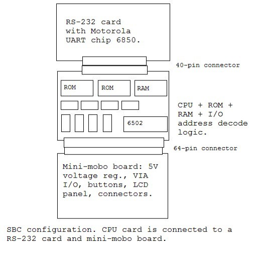
When
inserted into motherboard and EPROM reprogrammed accordingly, it will
be interfaced to other components connected to computer buses and
components.
3.1. Reset circuit.

3.2. CPU clock circuit.
3.3. CPU signals and address decoding.
3.4. I/O decoding.
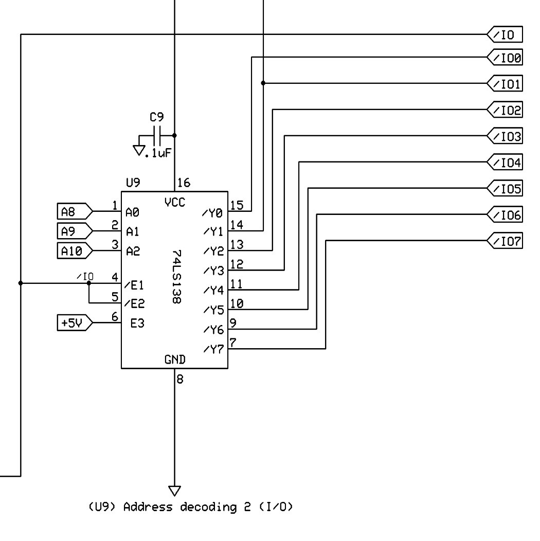
There will be 8 designated for I/O address spaces, 256 bytes each. Seems excessive at first, but considering that system should be highly expandable and that 4 of these slots will be already allocated for internal built-in system features like interrupt controller, banked RAM, RTC and VIA, it does not seem that excessive anymore. Also, 256 bytes for each I/O device seems much over the board, however it simplifies the decoder design.
3.5. Base RAM
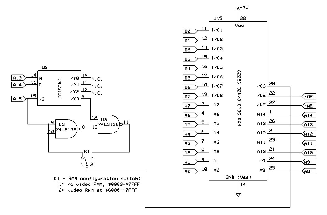
System
needs some RAM in the known address space, even if we don't use all
of it. I decided for 32 kB in the lower portion of the address space
(typical for MOS 6502, since stack and zero page are on the bottom
and reset and other vectors are on the top, RAM must be on the bottom
and ROM must be on the top). Part of that space may be used by
optional Video Card, selectable with the K1 memory configuration
jumper. The base RAM chip will not be selected in this case when
address is in Video Card address range, so a separate decoder can
select the Video RAM. That separate decoder would be basically a
clone of the 74LS139 circuit as seen below, reproduced on the Video
Card and output /Y3 would be the /CS signal for Video RAM OR the
signal from base RAM circuit could be used.
3.6. EPROM.
4. Control panel.
Control panel will provide basic controls to operate the computer system. Operator will be able to power the system on and off, reset the system and monitor/control parameters of the system via programmable keys and LCD display. The control panel will be connected partially to CPU bus and with additional cable connector to the CPU card for I/O signals (LCD, keypad).
5. RAM expansion card.
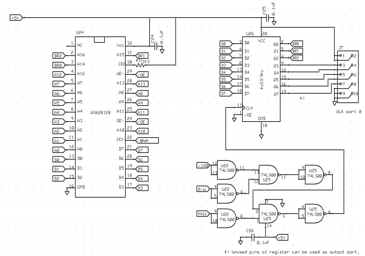
RAM expansion card will be connected to one of the CPU bus slots. It will consist of RAM bank switching register and RAM itself.
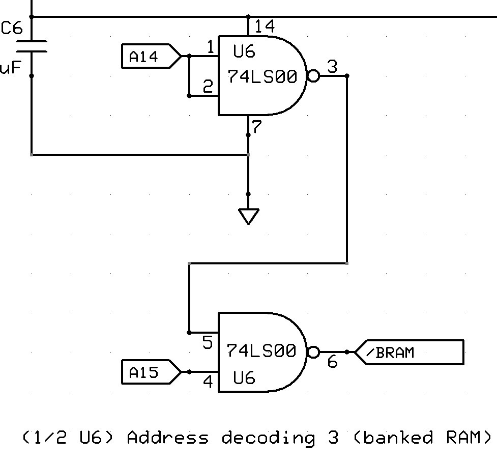
Signal /BRAM generated on the CPU card and put on the CPU bus, pin A30 will be used as Chip Select for RAM.
A 128 kB RAM will be available in 16 kB space by the means of bank switching (see Memory Map).
6. Real Time Clock.
RTC will be built on the same card as banked RAM expansion circuit to save space/CPU bus slots.
Based on DS1685 connected to 6502 bus without hardware latch, by the means of HW+software simulation, based on Chris Ward design.

7. Video Controller.
Video controller card will be based on Motorola MC6847 VDG (Video Display Generator) chip and will be designed as a CPU bus card. The card will have 8 kB of fast video RAM on board. Access to video memory by CPU and by VDG will be realized simultaneously in the opposite CPU clock phases. Video will be enabled by jumper switch on the CPU card, which will disable /CS signal for Base RAM in the video designated address range thus allowing video memory control in that range. The address space reserved for video (with jumper set to enable) will be $6000 - $7FFF (see Memory Map). This is 8 kB address space. However MC6847 requires only 6 kB of RAM in the highest resolution video mode. Therefore the address decoding circuit on board of Video Controller Card will select video RAM in range $6000 - $77FF and video mode control register in remaining space $7800 - $7FFF, thus enabling to use this space to both manupulate video RAM and control video modes.
If I wanted to use remaining part of video RAM for custom characters generator, things will get complicated. An extra I/O slot would be needed to control video modes. Alternatively, some PIA/VIA port pins can be used, but then I'd have to put PIA or VIA chip on the same board as video card. Not an elegant solution since some of the ports/pins of the VIA will be used for other purposes than VDG video modes.
Alternatively, I have been considering more modern options for video controller, including solutions build with modern micro-controllers or standalone boards. Depending on difficulties I encounter implementing originally intended solution I may switch to one of the alternative options for prototyping purposes or even permanent implementation.
Software.
Software will be designed layer by layer. The highest layer is a logical video device layer and programming API which will implement functions like printing characters to the device, querying video capabilities, turning on and off graphical modes, setting colors, turning the graphical pixels on and off, maintain the state of text and graphical cursors etc. The hardware device driver will implement the operations on the chip registers level necessary to accomplish fuctions requested by programming interface.
8. Sound Card.
Thinking about SID or Yamaha chip.
9. Mass storage.
Almost every generic purpose computer needs some sort of mass storage for data and applications. From the programming perspective, I am thinking of creating a high-level programming API that allows to access files logically (open, close, read, write, save, load) and the go down to intermediate layers that implement the structure of my file system (file system level), allow to read/write more elementary portions of data (like blocks) to/from the mass storage to/from the internal memory buffers etc. (logical device level). At these levels, it is yet not important what will be the hardware implementation at the hardware device level. Once that portion is designed, the hardware driver will take care of the physical data manipulation on the hardware device level.
The file system part can be designed as minimalist and as simple as possible OR I can choose to be fully FAT compatible to be able to freely copy data between IBM PC compatible computers and my system using the medium of choice. I am thinking something in between – implement a minimalist FAT protocol which will only be able to read and write to one single continuous file (FS image) on the storage medium. Inside that single continuous file, the structure of my file system will be implemented. This way I will avoid necessity of studying and reverse engineering the FAT file system structure, as I will implement my own FS instead. The down side of this solution will be that I will have to develop a software for IBM PC computer to be able to transfer files from/to my FS image. Not really a downside for me as I like implementing the software part even more than hardware part.
For hardware implementation of mass storage, I have been considering various options for MKHBC-8-Rx.
- Floppy drive/diskette.
Obsolete by today's standards (but that's the goal of this project to build a retro-style computer) and may be difficult. Luckily, I have a IBM PC compatible 3.5" floppy drive and plenty of 3.5" floppy disks.
- IDE hard drive.
The electronics/interface should not be too complicated.
- Solid state.
This is probably the best option based on solutions available today, but not fully in the spirit of the retro design that I originally wanted. However this project is moving slowly enough for me to adjust and change my design goals on the way. Therefore currently I am seriously considering this option as the mass storage for my retro computer.