What is an RTC?
The heart of this clock is a battery-backed RTC chip. Real-Time Clock (RTC) is a type of interface chip that is responsible for the timekeeping of the system. An RTC with a battery-backed feature means the chip has a separate power source for the chip to keep the time when the main power fails, which means I don't have to set the time again every time I unplug it.
DS1302 Trickle-Charge Timekeeping Chip
There are many choices of RTC chips available on the market today, I have decided to use DS1302 for many reasons:
- A cheap, well-known chip that is widely available.
- Uses SPI protocol to communicate which is very easy to control with logic chips. (More on this later.)
- Has all of the timekeeping features I need: Year/Month/Day/Date/Hour/Min/Sec.
- Data output is in a BCD format, which is ideal for a 7-segment decoder chip.
- Has a burst I/O feature. (More on this later.)
- Available in DIP package.
- Has a battery-backed feature. This chip could also trickle-charge a rechargeable battery by itself (but I use a single-use battery so I leave it disabled).
Datasheet is here: https://datasheets.maximintegrated.com/en/ds/DS1302.pdf
How should we make it tick?

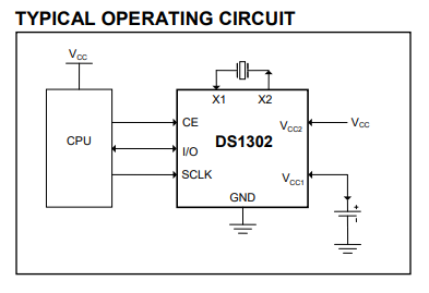
First is the block diagram. We can see that we need to:
- Connect the main power source to VCC2 pin.
- Connect the secondary power (backup battery) to VCC1 pin.
- Connect the ground pin (obviously).
- Connect a quartz crystal between the X1 and X2 pins. Noted that from the datasheet we will know that we need a 32.768 kHz crystal with a 6 pF load capacitance value.
- Connect the SPI bus to the remaining 3 pins. Noted that this chip shares the SPI MOSI and MISO pins. This will be very important later.
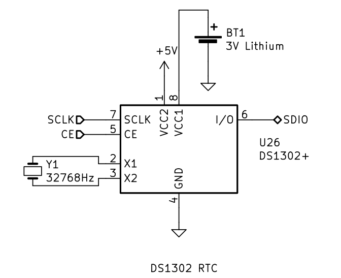
So now we have this circuit below:
Note: I do include 100nF decoupling capacitors at every Vcc pin on every chip, but I put these all in the power input sheet, so they will not show on the pictures.

Communications


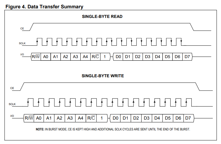
Communications with the chip use a common SPI protocol. First, we drive the chip enable (CE) high, then we feed our clock signal in the SCLK pin, and read/write the data on the I/O pin. However, from the datasheet there are some important points:
- The first byte we send to DS1302 is a command byte, which tells which register and region to read/write from and if this command is a read or write command.
- DS1302 will switch from read to write mode automatically after 8 clock pulses if the command we send is a read command.
- The data going in/out of the chip is LSB-first.
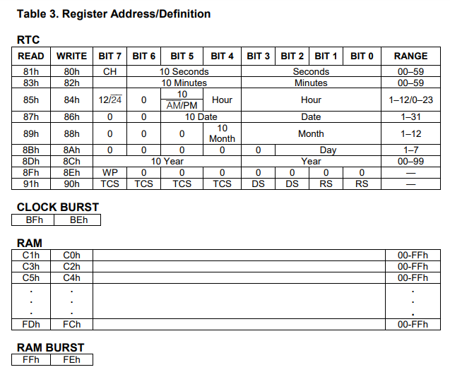
- The data stored on the chip are organized into a set of 8-bit registers. We can read or write a specific register, or we can access full date-time data in one go by issuing a clock burst command.
- A clock burst command, when issues on the clock bank, will output full 8 bytes of time data and 1 extra byte that contains a write protect (WP) bit indicating if we could write to the chip or not.
- We need to clear the WP bit by writing 0x00 to 0x8E register before we could write anything to the chip.
From what we gathered from the datasheet, to build an MCU-Less clock based on this chip we would need to have the following:
- An SPI clock source
- A sampling clock source (to query time from the chip)
- A CE signal controller
- An SPI bus I/O direction controller
- An SPI bus arbitration controller (to make sure commands are executed in a correct priority and did not interfere with other commands)
- A place to store DS1302 clock burst read (0xBF), clock burst write (0xBE), and WP write (0x8E) command bytes
- A place to store time data we got from the chip
- A place for the user to input new time data (plus related control logic)
- A place for the user to clear WP bit
- A way to make sure everything starts up correctly when powered-up (POR reset)
- A display that will show the date-time data
- A power source
- And other misc logic features
You can see there's quite a lot to do, which I will write about them in the next log.
Thanks for reading! :D
 Sleepy Pony
Discussions
Become a Hackaday.io Member
Create an account to leave a comment. Already have an account? Log In.