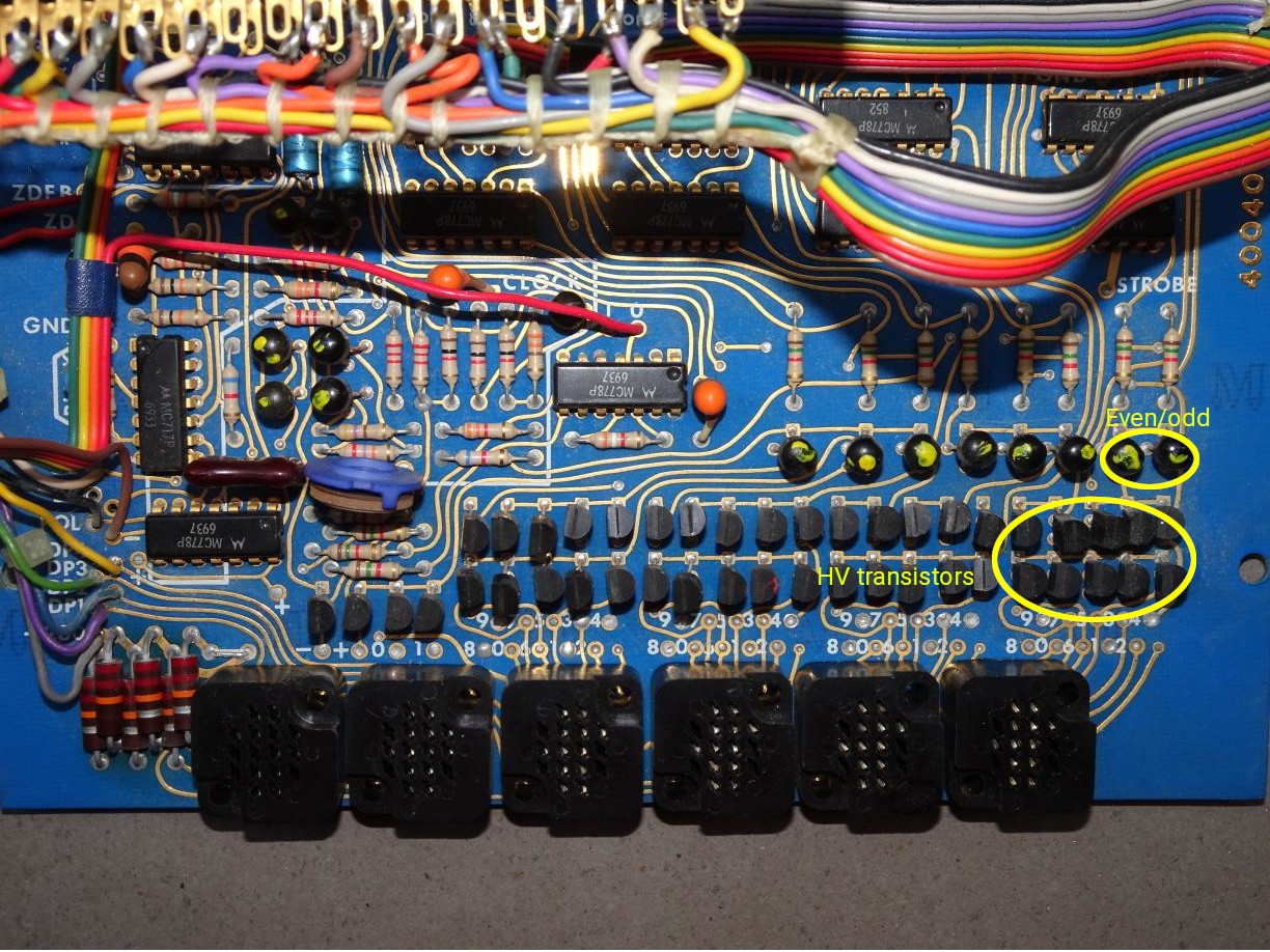
Now I have to work out how the nixies, which are 1 of 10 indicators (ignoring the decimal point) are driven from binary inputs. So I examined the driver transistors and the display latches feeding them using optical trace scanning (my eyes 😉) and a continuity meter.

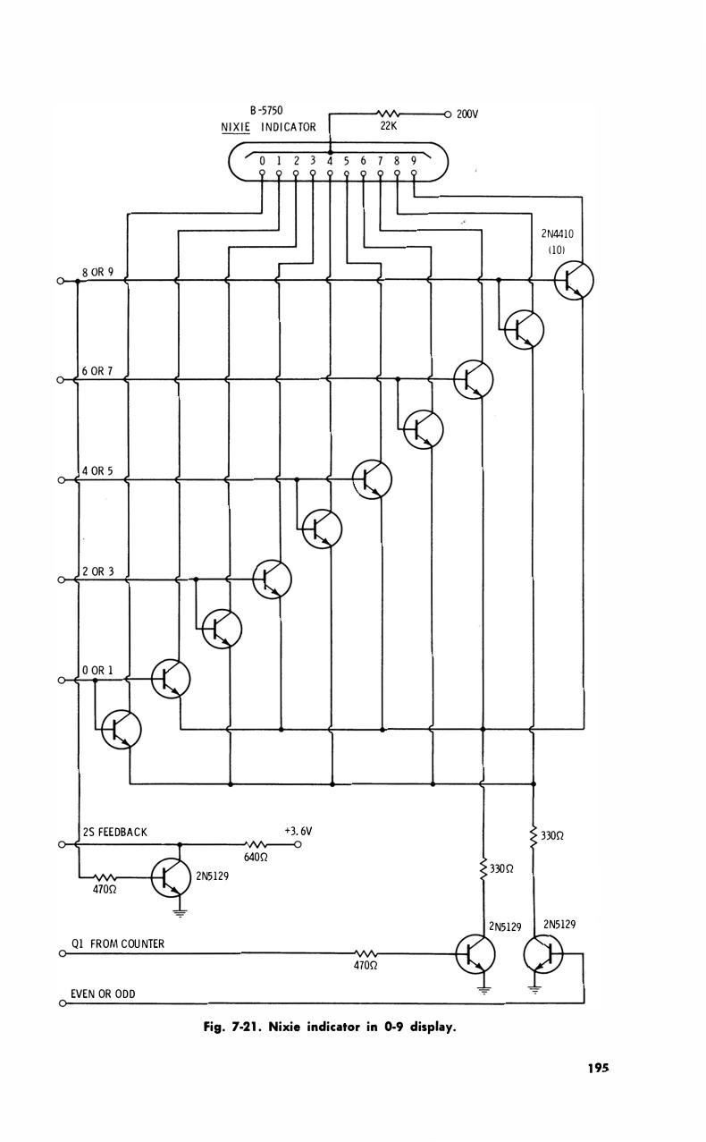
Each nixie is driven by 10 transistors grouped 5x2. Each pair of 5 pairs has bases wired together. The reason will be evident in a moment. The circuit is pretty much similar to the following page I have excerpted from the RTL Cookbook I fetched. So instead of 4 binary inputs weighted 1-2-4-8 as we would expect nowadays, there are 6 inputs. The first is the even/odd line, and the others are the 0/1 2/3 4/5 6/7 and 8/9 inputs. So for example to display a 7, the odd input is active and the 6/7 transistors are driven but only one will conduct, the one whose emitter is grounded by the odd driver transistor.

Tracing the inputs of the transistors from the MC778 chips reveals that two 2N5134 transistors switching between even and odd digits are driven in antiphase from one flip-flop using the Q and ~Q outputs. The 5 other flip-flops drive the 5 pairs of 2N4409 high voltage transistors. These 6 flip-flops contained in 3 MC778 chips, and there are 4 columns of 3, for the rightmost 4 digits. We'll ignore the leading 0/1 and the +/- nixies for now.
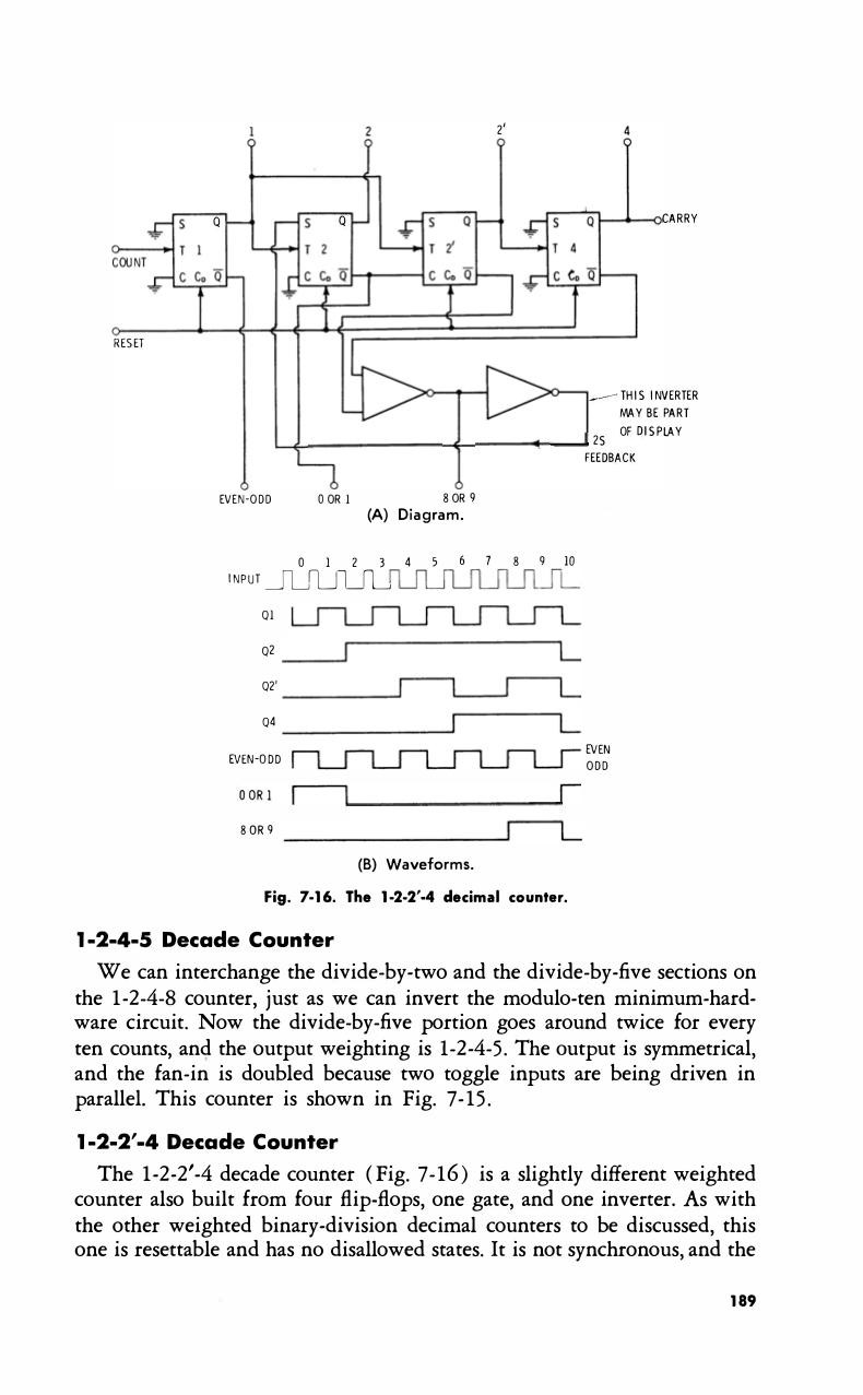
How does one get from a BCD counter to this biquinary code? The RTL Cookbook provides one answer. The counter stage is not a 1-2-4-8 scheme, that requires too much decoding. Instead it is probably a 1-2-2'-4 scheme shown in the next diagram. By the use of a few extra gates this is converted to a biquinary code. So the "comms board" I showed earlier is most likely a code converter board. It contains multiple MC717 NOR gates and the wiring loom goes to the main board near the flip-flops discussed.

There is another small mystery. There is no current limiting resistor on the bases of the 2N4409 HV transistors. This means that the design is relying on the collector pullup resistor of the RTL flip-flop to limit the current. The nominal value given in the datasheet is 3.6k. With a voltage supply of 3.6V and a B-E drop of 0.6V, this means a bit less than 1mA current drives the HV transistors. That is plausible. But there is another question: doesn't this load down the high level of the flip-flop so that it's not a true 1? Yes it does, but as the flip-flops are used as buffer latches and the outputs don't drive other RTL logic gates, this has no consequences. Obviously the designer did this deliberately and saved quite a few resistors this way. 👍
 Ken Yap
Discussions
Become a Hackaday.io Member
Create an account to leave a comment. Already have an account? Log In.