 Dave Collins
I'm nearing completion of the clock module for the prototype and the eventual build. This has 3 main goals:
- No 555 timer. (honestly if your module has a inverter why use a 555).
- Latch both CLK & ~CLK save the state through a halt and resume sequence.
- support a HLT on a HIGH signal from the CPU.
I completed a first draft of what I'm building in EasyEDA. I have tested most of the module and it works well. I will need to do further refinements to get it dialed in but its about 90% so I've uploaded a PDF of the working schematic. You can find it in the files section.
If you want a latched clock why no 555?
To be honest; I don't really have a good answer beyond its been over done a million times. I had initially thought to build a op-amp oscillator but, opted (heh) to do an R-C inverter instead. The reason is simple; if your non-crystal clock design has an inverter, you should not use a 555, at least in my opinion.
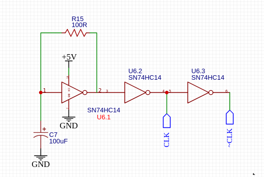
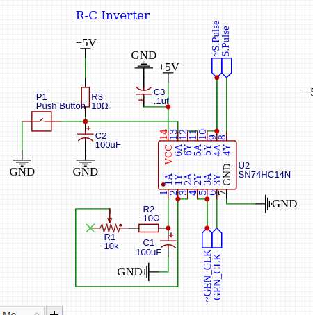
Here is a over simplification of the clock's main astable oscillator. The first stage takes the RC oscillation (which appears on the scope as a triangular wave mostly; and outputs a result witch is more or less a rhomboid (and inverted). Since a waveform that is more or less a parallelogram is going to cause a problem for CMOS High levels, we feed this through a second stage, which flattens out the transitions and we get a nice square wave. The third stage is more or less just to get a inverted clock, although extra buffering is always nice on the thing you are going to hook to nearly every IC on your build. With 2 passives ( three when we wire in a trim pot), and 3 more inverters on the other side of the package to de-bounce a single step you can't really go wrong Full R-C Inverter Clock, with single pulse de-bounce.
In many, many, MCU's with internal oscillators this simple R-C and invert tactic is used. it produces a fairly decent nearly 50% duty cycle, though honestly this can be further refined. Another advantage to building the clock this way is we get full control of the added ~CLK signal off the output latch. By way of comparison, the ~Q output of the 555 timer latch is tied to an internal transistor in, and essentially discharged off to the ground.
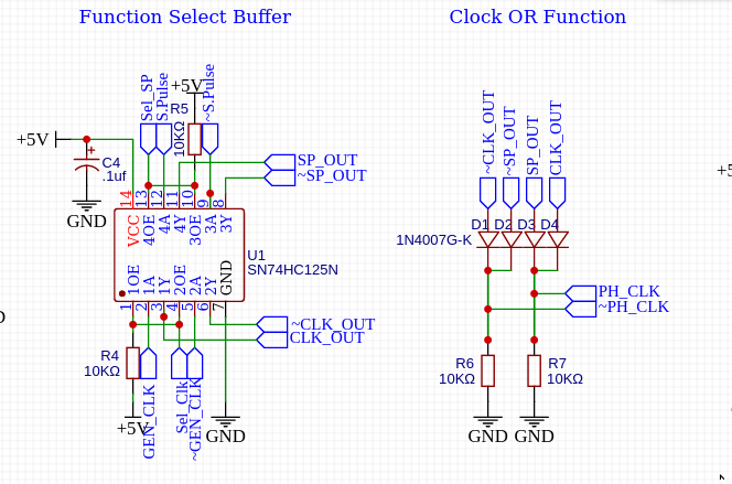
We can control the clock selection through a quad buffer (two sets for both ~CLK, CLK, Single Pulse, and ~Single Pulse), and a switch we de-bounce, elsewhere in the circuit. We tie the outputs together using a simple Diode/Resistor setup, in this case only, it's OK to leave the output of the tri-state buffer in tri-state as the OR gates are tied low on their outputs and do not actually care the difference between high Z and 0v (I think). I build the OR gates this way as two gates from diodes use slightly less tracks, and fewer power rails than a package with two terminated gates, which being in the clock module will likely not find use.
A second buffer takes the combined clock pulses to and from halt with a high pulse else-ware in the CPU; It's highly likely this part of the circuit will change drastically. I really don't like half using a package like this. It's possible I could bring the CPU to halt by grounding out both R-C circuits similar to the way James Cameron did in his pipeline CPU build; perhaps somebody who's taken the time to read all of this has a better idea?
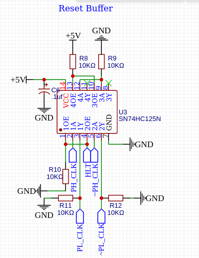
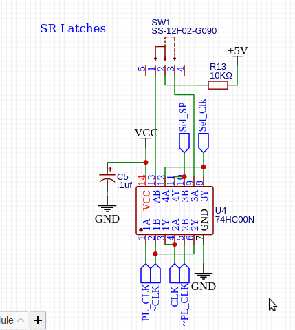
The S-R latch brings it all together in the end. One side of the Quad NAND gate handles the S-R latch for the clock, and the other handles the de-bounce for the switch that picks single pulse or the clock. I still have yet to build the HLT signal in place however, I get good oscillation out of the latch. I run into issues where the latch occasionally enters an unknown state brought on by both ~CLK/CLK being in full cut off. I have yet to figure this part out, i suspect the latch is oscillating at a very high rate but I require further testing. Additionally my tiny portable scope is more for automotive applications, so does not have a very high sample rate. After I have a finished prototype clock module that's fully built I will post a video.
I am entering day three of unsettling unknown upper-respiratory viral infection, and so working on my laptop is generally the limit of what I can do right now, they tested for COVID but my results on the longer test haven't come back yet so I am stuck at home while we verify. And so i don't get co-workers and family members sick, I am isolating away from my work bench (which i doubt I'd have the mental clarity to work at in any case).
Hopefully you found my ramblings entertaining or interesting at the very least. I rattled off a lot of self-taught nonsense in the above; so take that with a huge grain of salt. If anybody is willing to set me straight; or tell me my design is rubbish and how, to fix it I am all ears. Have a great week everybody :)
Discussions
Become a Hackaday.io Member
Create an account to leave a comment. Already have an account? Log In.