Before I can really get into the design, I need to understand the basics of the 555 timer. Although I’ve worked on a handful of projects, I’ve yet to implement one in my designs (hopefully this project will resolve this trend).
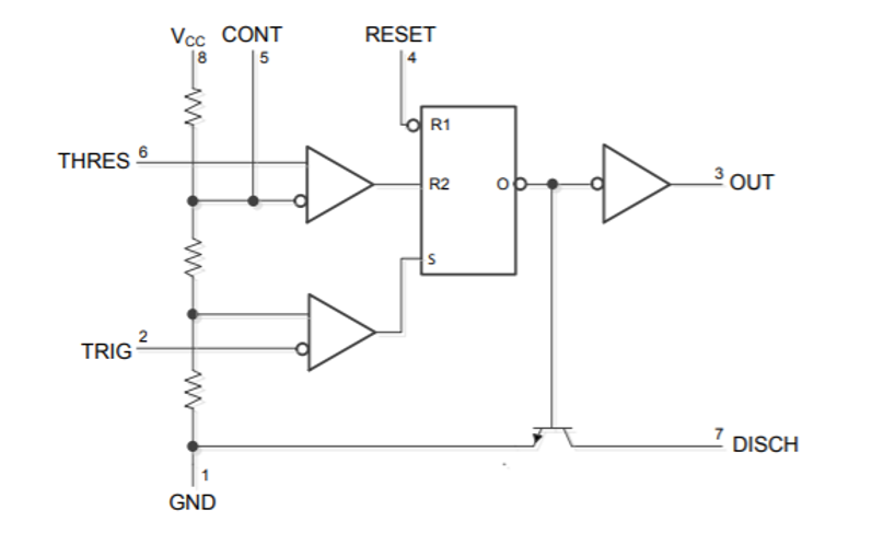
The simplified schematic for the chip is shown below. Internally the 555 primarily contains some comparators, an SR latch, a buffer, and a discharge transistor. That latch will definitely come in handy for gate design down the road.
For specifications, typical output sink/source is about 100mA, and a maximum output near 100kHz. Obviously, these parameters may shift depending on the manufacturer I choose.

 Jesse Farrell
Discussions
Become a Hackaday.io Member
Create an account to leave a comment. Already have an account? Log In.