 Jesse Farrell
Designing a D type latch (need this for my flip flop) using only 555’s was less trivial than I initially expected. The main issue was implementing the functionality of the enable signal. The latch could easily be brute forced using 5 or so 555’s but this would dramatically bloat the BOM.
The widget will need to store several bytes of data, using excess gates in these latches will dramatically increase the overall cost and footprint of the board. Therefore, some basic active components will be allowed for the D type latch. One good solution posted by Tim was to introduce a pass-through transistor and hold the THRES/TRIG pins at ½ VCC, see below.
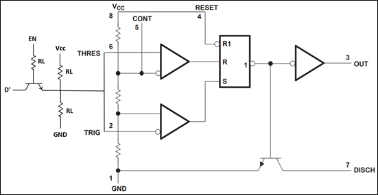
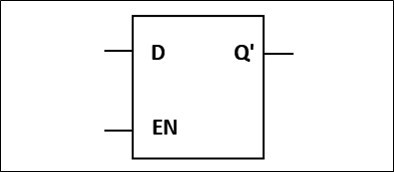
It’s important to note that the implementation above uses the inverted input D. Alternatively, we could think of this as taking in D and outputting Q’ see block below. Obviously, we can remove this inversion with an inverter, but we may be able to avoid this altogether when designing a flip flop. A small capacitor should be added to the emitter of the transistor to help stabilize the SR triggering.
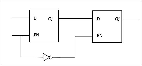
We can now create a flip flop by cascading two of these latches. Note that this flip flop will trigger on the falling edge of the clock signal, and the previously mentioned inversion solves itself.
*breadboarded this circuit at first but forgot to take captures, they'll be added likely later today (Jan 9th)*
Discussions
Become a Hackaday.io Member
Create an account to leave a comment. Already have an account? Log In.