 Colin
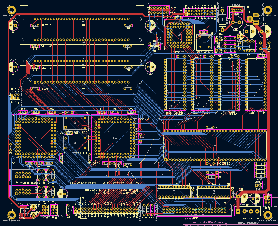
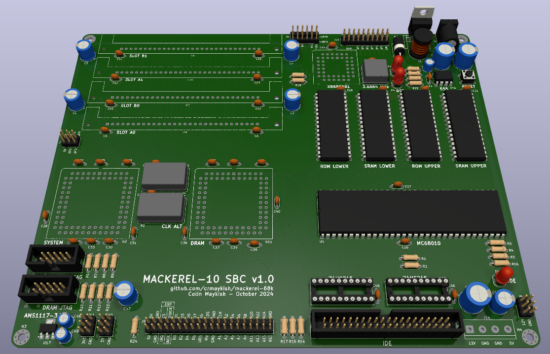
ColinIn my last couple posts, I described the DRAM controller and IDE interface I've been working on. With both features working reliably, it's time to combine them together and build an SBC. One element I did not consider when making the jump from the 68008 to the 68010 is how much more complicated the actual PCB routing would be with all those extra pins. The DRAM controller also adds a lot of complexity to the routing and takes up a lot of board space.
I designed Mackerel-10 v1 as a four-layer board with the same stack-up as Mackerel-08, signal/ground/power/signal. The circuit design is not drastically different than the prototype PCBs I've been working with until now. The main difference is the on board IDE header and the addition of two extra SIMM slots. I wanted the option to use 4x4MB DRAM.
I also broke out more I/O from the DUART and more power pins in general. I decided to keep the system expansion header limited to an 8-bit data bus with A1-A15 exposed, plus enough control signals to attach reasonable I/O devices. It did not feel necessary to expose the full 16-bit data bus or all of the address pins when most of the address space will be filled with on-board DRAM anyway.
Finally, I added an optional second clock oscillator to both the system and DRAM CPLDs. I'd like to experiment with running the DRAM state machine on its own clock in an attempt to maximize both the CPU speed and the DRAM access efficiency.
This is the biggest and most complex board I've routed so far. PCB manufacturing prices don't increase that substantially as the board size grows, so I did not go crazy trying to keep it as small as possible. It ended up being 210x170mm.
Discussions
Become a Hackaday.io Member
Create an account to leave a comment. Already have an account? Log In.