Mackerel-10 now has a functioning DRAM controller and a serious boost to its total RAM in the form of two 4MB 30-pin SIMMs. With the 1MB of onboard SRAM, this brings the total usable memory to 9MB. Adding DRAM to any homebrew project always felt to me like a major milestone on the way to building a “real” computer. While it’s a long way from the complexity of modern DDR, it’s a significant step up in both complexity and capability compared to stacking a bunch of SRAM together (e.g. Mackerel-08).

I’m hardly the first person to add DRAM to a 68k system and I want to call out and thank a few projects I found to be terrific references while I was putting this together:
- Lawrence Manning's MINI020 (and the rest of his 68k projects)
- Tobias Rathje's T030
- Stephen Moody's Y Ddraig
All three projects implement some form of DRAM with a 68k CPU and I borrowed liberally from their implementations and write-ups. Thanks for sharing!
The best decision I made while working on this was definitely taking the time to setup a Verilog testbench to simulate my implementation before trying to debug it on real hardware. In fact, I wrote the controller and simulator before I had any design for the hardware. Seeing the Verilog behave as I expected gave me a lot more confidence in my PCB design and saved a ton of time during board bringup.
There are plenty of testbench tutorials out there and this is not one of them, but I used iverilog and GTKWave to simulate my design. Although I’m building and flashing the CPLD with Quartus (which includes ModelSim), I’d rather not spend a second longer than I have to in that program.
There are two areas that make dynamic RAM more complicated to deal with than static RAM. The first issue is that the address pins on the SIMMs are not all exposed as they are on SRAM. Instead, they are multiplexed into rows and columns. This means that reading and writing data is no longer as simple as putting the full address on the bus. The basic read cycle for DRAM looks like this:
1. Split the 24 bit address bus of the 68000 into row and column addresses (11 bits each in the case of 4 MB SIMMs)
2. Write the row address to the SIMM’s address pins and assert the RAS (row address strobe) line
3. Write the column address to the SIMM’s address pins and assert the CAS (column address strobe) line
4. Read or write the resulting data
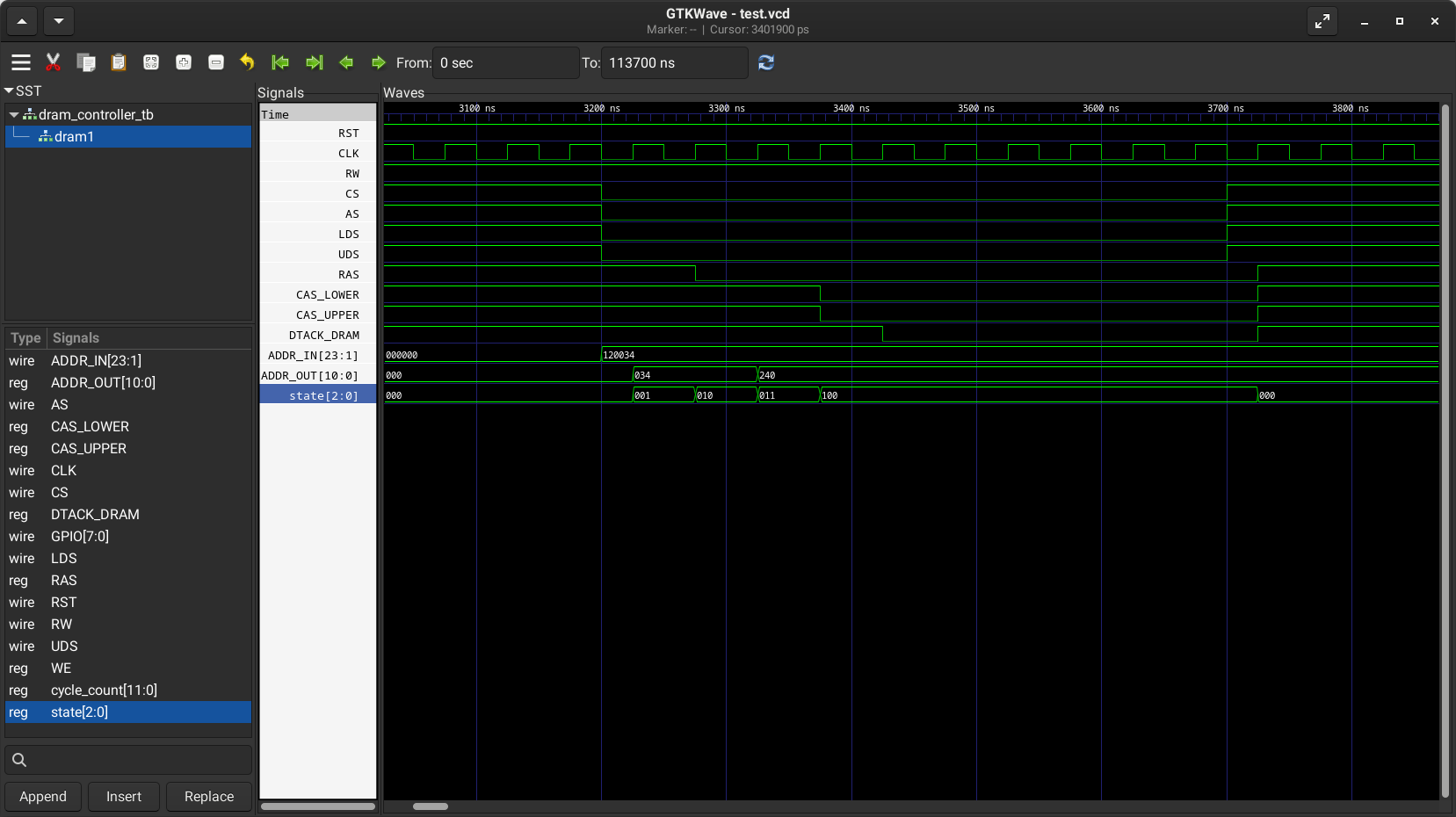
Conceptually not too difficult to comprehend, but care has to be taken to meet the timing requirements at each one of these stages. My implementation handles this with a finite state machine. Each step in the DRAM cycle corresponds to one or more states in the FSM. Here’s what this read cycle looks like in simulation:

Once the DRAM responds with valid data, the controller will bring DTACK LOW and hold the data on the bus until the CPU brings the AS line HIGH, ending the memory cycle. This hold time is exaggerated in the simulation. A write cycle is almost identical except the WE pin on one or both SIMMs is asserted.
The other challenge involved in using DRAM is the need to constantly refresh the memory cells. Every cell in the array has a maximum amount of time it can hold a value before decaying (DRAM is just a giant grid of capacitors). Refreshing a cell means reading it and immediately writing it back to restore the charge in the capacitors. Fortunately the DRAM chips provide a few ways to deal with this. The method I chose is CAS-before-RAS refresh. In a normal memory access cycle, RAS is asserted and then CAS is asserted. If the reverse is done, the DRAM will run a refresh instead. The DRAM chips are also kind enough to maintain internal addresses for the next refresh target, so all we have do is run a refresh cycle frequently enough to keep all of the cells topped off.

Here you can see the relatively simple process of asserting CAS and then RAS. Each address has to be refreshed roughly every 16ms, so the frequency of the refresh cycle will depend on the total size of the DRAM. The state machine ensures that a refresh cycle takes precedence over a normal memory access cycle, so occasionally memory access by the CPU will be delayed slightly until the refresh is finished. This is not noticeable in normal operation, but it does technically slow down the system ever so slightly. That’s the trade-off for massively higher memory density compared to SRAM.
With all of this extra RAM, Mackerel-10 was ready to boot uClinux for the first time. Some minor updates to the bootloader and the kernel’s memory map were required, but Mackerel-10 now runs Linux. It’s great to see the kernel with all of that free memory - so much room for activities.

 Colin M
Discussions
Become a Hackaday.io Member
Create an account to leave a comment. Already have an account? Log In.