Getting a DRAM controller working at all feels like a great accomplishment, and while it has been stable and functional, there were some situations I couldn't explain. For example, it was not possible to run the DRAM controller at anything other than twice the CPU speed, even running them at the same frequency failed completely. I was not satisfied with my understanding of my own design. I also wanted the option to run the DRAM on its own independent clock to completely free up the choice of oscillator for the CPU.
With the goal of better understanding and more flexibility, I took the lessons learned from my first iteration and went back to the drawing board, starting with the datasheet. The simplest place to start is the CAS-before-RAS refresh.
CAS-before-RAS Refresh

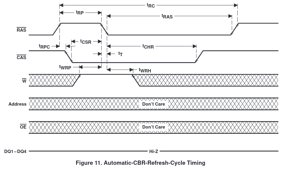
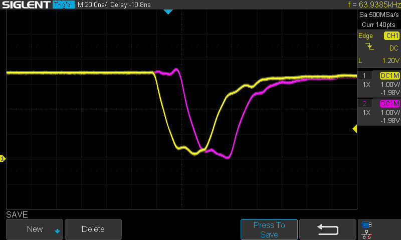
The refresh process is not complicated: pull CAS low, then pull RAS low, raise CAS, and then raise RAS again. One thing worth noting here is that the WE pin has to be HIGH by the time RAS is lowered. Since the state of the WE pin is "don't care" for the rest of the refresh cycle, I chose to pull it HIGH in the first state of the refresh state machine. Note: Mackerel-10 has four 30-pin SIMMs in two 16-bit pairs, A and B. RAS is shared between SIMMs in a pair, but the CAS lines are all independent, thus two RAS pins and four CAS pins in my controller.
REFRESH1: begin
    // Acknowledge the refresh request
    refresh_ack <= 1'b1;

    // Lower CAS
    CASA0 <= 1'b0;
    CASA1 <= 1'b0;
    CASB0 <= 1'b0;
    CASB1 <= 1'b0;
    WRA <= 1'b1;
    WRB <= 1'b1;
    state <= REFRESH2;
end

REFRESH2: begin
    // Lower RAS
    RASA <= 1'b0;
    RASB <= 1'b0;
    state <= REFRESH3;
end

REFRESH3: begin
    // Raise CAS
    CASA0 <= 1'b1;
    CASA1 <= 1'b1;
    CASB0 <= 1'b1;
    CASB1 <= 1'b1;
    state <= REFRESH4;
end

REFRESH4: begin
    // Raise RAS
    RASA <= 1'b1;
    RASB <= 1'b1;
    state <= PRECHARGE;
end
The final piece of the DRAM refresh cycle is determining how often it needs to happen. According to the datasheet, all 2048 rows need to be refreshed every 32 ms. If we refresh each cell incrementally with CBR, that means we need to refresh a cell every 32 ms / 2048 = 0.015625 ms. That equates to 64 kHz. Finally, the DRAM controller is running from a 50 MHz oscillator, so 50 MHz / 64 kHz = 781 cycles between refreshes.
The Verilog for counting cycles is basic, but I'll include it here for reference. The two refresh_ registers are used to pass the refresh state back and forth between this generator code and the main state machine. REFRESH_CYCLE_CNT is set to 781.
// ==== Periodic refresh generator
reg refresh_request = 1'b0;
reg refresh_ack = 1'b0;
reg [11:0] cycle_count = 12'b0;

always @(posedge CLK_ALT) begin
    if (~RST) cycle_count <= 12'b0;
    else begin
        cycle_count <= cycle_count + 12'b1;

        if (cycle_count == REFRESH_CYCLE_CNT) begin
            refresh_request <= 1'b1;
            cycle_count <= 12'b0;
        end

        if (refresh_ack) refresh_request <= 1'b0;
    end
end

Read/Write Cycles
With the CBR refresh behavior confirmed, I started to revamp the rest of the state machine, i.e. the process of actually reading and writing memory. As mentioned, my first implementation worked, but just barely. One of the issues I had was a dozen or more compiler warnings in Quartus that looked something like this: Warning (163076): Macrocell buffer inserted after node. I could not track down an exact cause, but the little information I found online and my own testing seemed to indicate that this error basically means "you're trying to do much work at once". By breaking up my state machine into more smaller states and removing highly parallel pieces of code, I was able to get rid of all all these warnings. It seems like the key is not to change too many register values per clock cycle, but to instead pipeline the design.

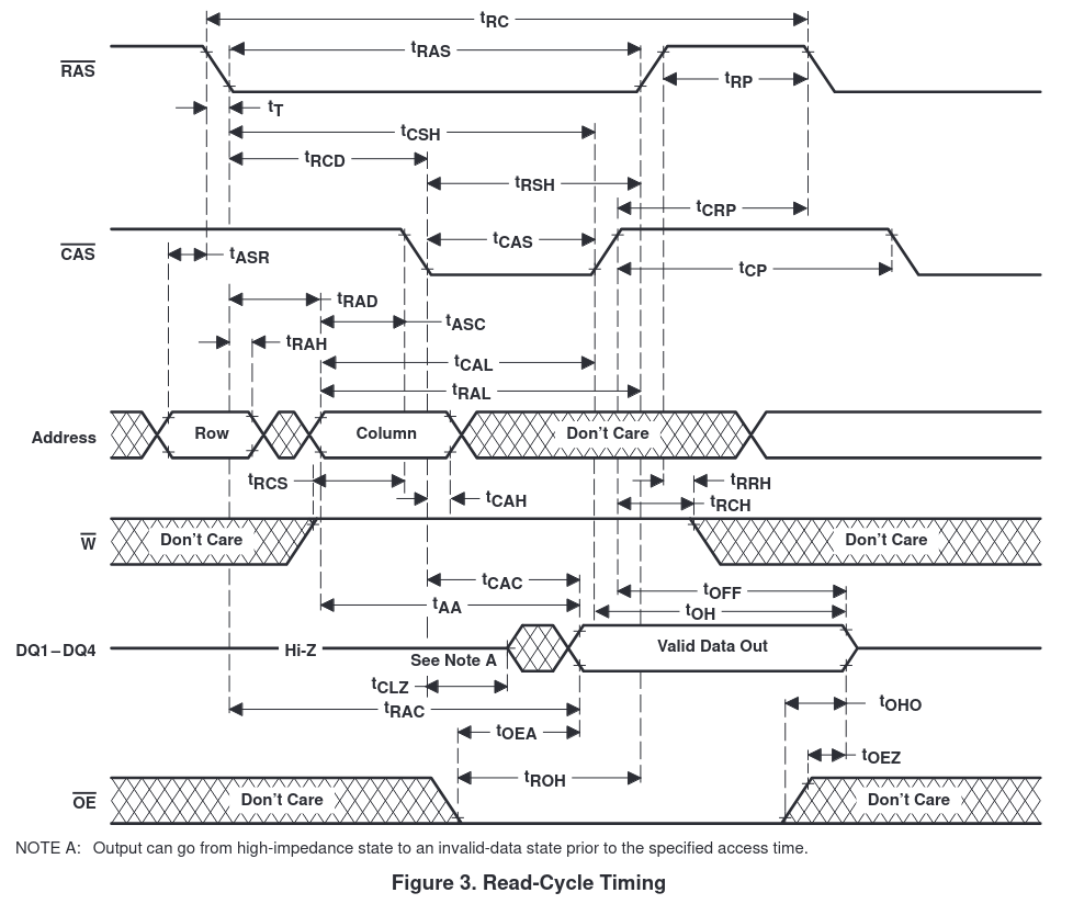
The actual logic of the DRAM read and write cycles hasn't changed. It's still a multi-step process where the controller multiplexes the CPU address bus to the row address of the DRAM, asserts /RAS, multiplexes the column address, then asserts /CAS and /DTACK until the CPU finishes the bus cycle. Here's a snippet of the state machine showing this piece:
IDLE: begin
    if (refresh_request) begin
        // Start CAS-before-RAS refresh cycle
        state <= REFRESH1;
    end
    else if (~CS2 && ~AS2) begin
        // DRAM selected, start normal R/W cycle
        state <= RW1;
    end
end

RW1: begin
    // Mux in the address
    ADDR_OUT <= ADDR_IN[11:1];
    state <= RW2;
end

RW2: begin
    // Row address is valid, lower RAS
    if (BANK_A) RASA <= 1'b0;
    else RASB <= 1'b0;
    state <= RW3;
end

RW3: begin
    // Mux in the column address
    ADDR_OUT <= ADDR_IN[22:12];

    // Set the WE line
    if (BANK_A) WRA <= RW;
    else WRB <= RW;

    state <= RW4;
end

RW4: begin
    // Column address is valid, lower CAS
    if (BANK_A) begin
        CASA0 <= LDS;
        CASA1 <= UDS;
    end
    else begin
        CASB0 <= LDS;
        CASB1 <= UDS;
    end
    state <= RW5;
end

RW5: begin
    // Data is valid, lower DTACK
    DTACK_DRAM <= 1'b0;

    // When AS returns high, the bus cycle is complete
    if (AS) state <= PRECHARGE;
end
And here's what it looks like in simulation:

There are more stages than in my previous version, but each stage is doing a small and obvious thing. It's tempting to try to combine some of these steps together, and there's probably room for optimization, but clarity and stability are the priorities at the moment.
Crossing Clock Domains
The final piece I wanted to tackle was having the ability to run the DRAM controller at any speed, not having it tied to a multiple of the CPU frequency. Because DRAM takes more cycles to access than SRAM, the whole system is slower clock-for-clock. It's not a dramatic difference, but those extra clock cycles add up. One way to alleviate some of this delay is to run the DRAM controller at a faster clock than the CPU. This shouldn't be too hard. Most 68000s are only rated to 10 MHz or so. The CPLD running the DRAM controller can easily handle 50 MHz. With this arrangement, most or all of the extra cycles taken up by DRAM access happen between the slower CPU cycles.
In a perfect world, this change would be as simple as connecting a second faster oscillator to the DRAM controller and updating the CLK pin. In reality, this leads to metastability. I won't try to explain that concept here as I'm just coming to terms with it myself, but the outcome is that there needs to be a bit of a handoff when referencing the slow CPU signals from the fast DRAM clock cycles. This is called crossing clock domains and it's accomplished by double registering the slower signals before using them in the faster domain. Fortunately, Mackerel only has two input signals that fit that description: CS and AS.
reg AS1 = 1;
reg CS1 = 1;
reg AS2 = 1;
reg CS2 = 1;

always @(posedge CLK_ALT) begin
    AS1 <= AS;
    CS1 <= CS;
    AS2 <= AS1;
    CS2 <= CS1;
end
Double-flopping the DRAM chip-select pin and the CPU's /AS pin like this virtually guarantees that the DRAM controller won't sample them during a transition (the cause of metastability). CS2 and AS2 are now nice and stable in the DRAM's clock domain and they can be used to kick off the DRAM access process (see the IDLE state in the Verilog above).
We've now removed the link between the CPU clock and the DRAM controller. This does not scale infinitely. There are some limitations on the differences between the clocks, but it's dramatically more flexible than my last attempt. In testing, I was able to run the DRAM controller at 50 MHz with the CPU clock anywhere between 9 and 20 MHz. It's also possible to remove the double-flopping and run on one synchronized clock, something I could not do previously.
Wrapping Up
Implementing a DRAM controller for a 40 year old CPU on a 20 year old CPLD is quite a niche subject, but this is the information I wish I had when I started working on this. Hopefully this is helpful to somebody. If that's you, share your project. I'd love to hear what you're working on!
Here is the full Verilog code for the DRAM controller: https://github.com/crmaykish/mackerel-68k/blob/master/pld/mackerel-10/dram_controller/dram_controller.v
 Colin M
Discussions
Become a Hackaday.io Member
Create an account to leave a comment. Already have an account? Log In.