 kelvinA
[Edit 1]
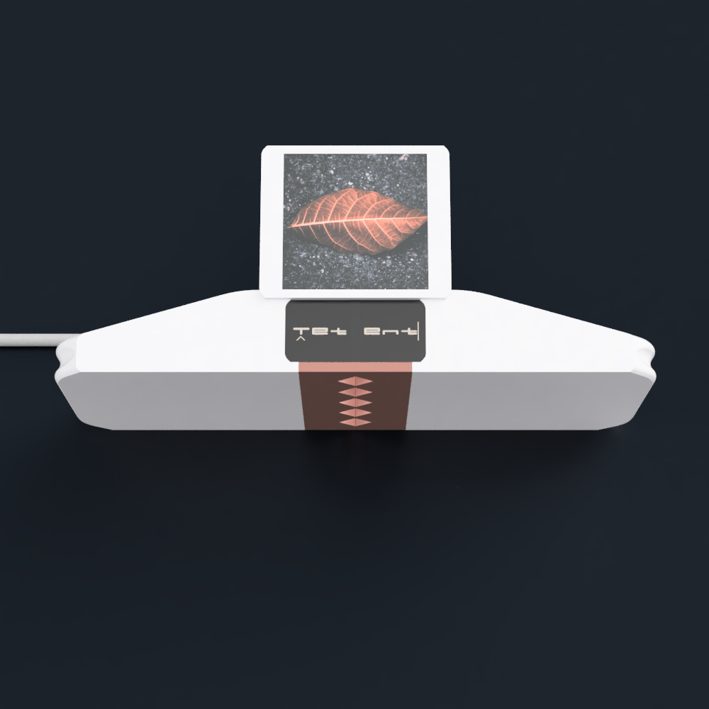
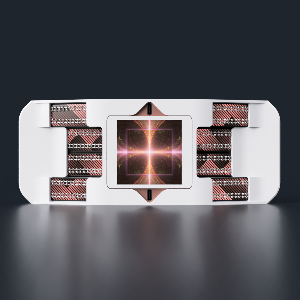
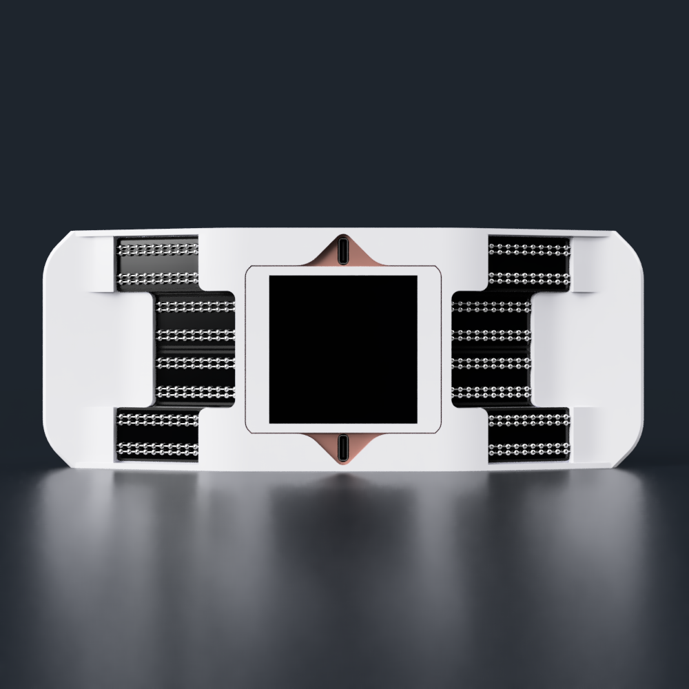
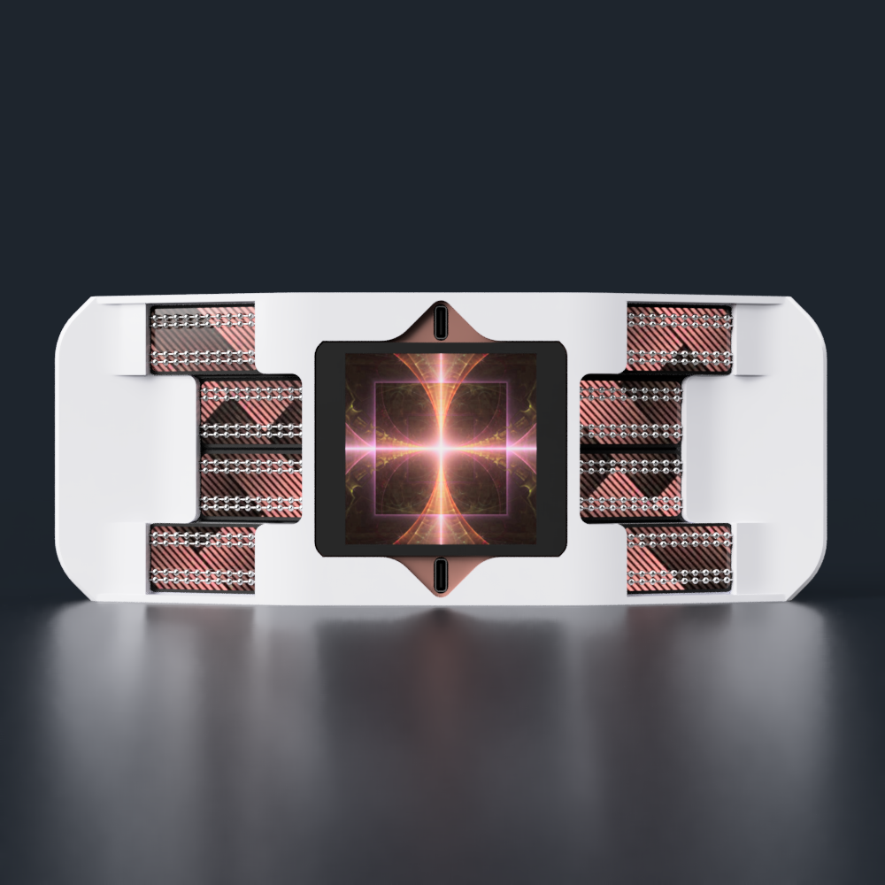
I've been staring at the design more, and I think I'll be going with the white bezels. The reason is because there's still much more white visible from Tetent itself than the bezels from the first person perspective, and the bezels themselves are much less obvious from the 3rd person perspective, allowing the design to have a centred, black square when all screens are off.
[Edit 1: End]
(reference to Apple's "Light. Years Ahead." tagline and a line Megumin said)
Internal features and software features are still quite likely to increase, but externally, I don't think there will be any visible changes from new features. I'm hoping the BOM is around the £300 range.
Speaking of internals, I've done some research on USB PCB creation, electromagnetic radiation and the pros/cons of 2 vs 4 layer PCB's, and I'll be playing it safe with the 4 layer PCB for both Tetrinsic and Tetent boards.
I'm also going to take advantage of each Tetrinsic having USB capabilities and just wiring one Tetrinsic to 1 port/device, and then having a selector similar to input selection menus on TVs. Right now, the selection would be [USB Port 1, USB Port 2, Internal SBC]. I'd need some way to toggle between using the port for Tetrinsic I/O and using it for SBC I/O.
I'd also like to mention that the FOV of the 1440px display is low enough that these cheap magnifying glasses (with led lighs) don't cause any annoying chromatic abberations of the content. The focal distance, which is a tad too short for laptop/desktop viewing distances, is right in the zone needed for this handheld mini-monitor. Additionally, since I don't have to look down occasionally for a mouse/keyboard, the potential chance of eye fatigue (from constantly changing focus) is reduced.
The only main concern now is: Will the solution fail, due to ergonomics?
I consider everything else from PCB creation to firmware programming to the mental overhead using this device as "Skill Issue". It is only if Tetent is damaging to my fingers where the solution will fail. Unfortunately, in these 15 months of research, I've noticed that the tolerance for an ergonomic solution is quite low. I guess that's somewhat expectable, since higher bandwidth electronic signals are usually less tolerant to PCB design imperfections too.
Discussions
Become a Hackaday.io Member
Create an account to leave a comment. Already have an account? Log In.