In the last couple of mounths I had some time to spend on the software side of the microscope and was able to achive very cool thing with it.
The first thing is I made an automated focusing method for it, which uses focus contrast search. It is very simly just stepping in Z till it finds the peak value of the sharpest contrast, like the below picture shows:
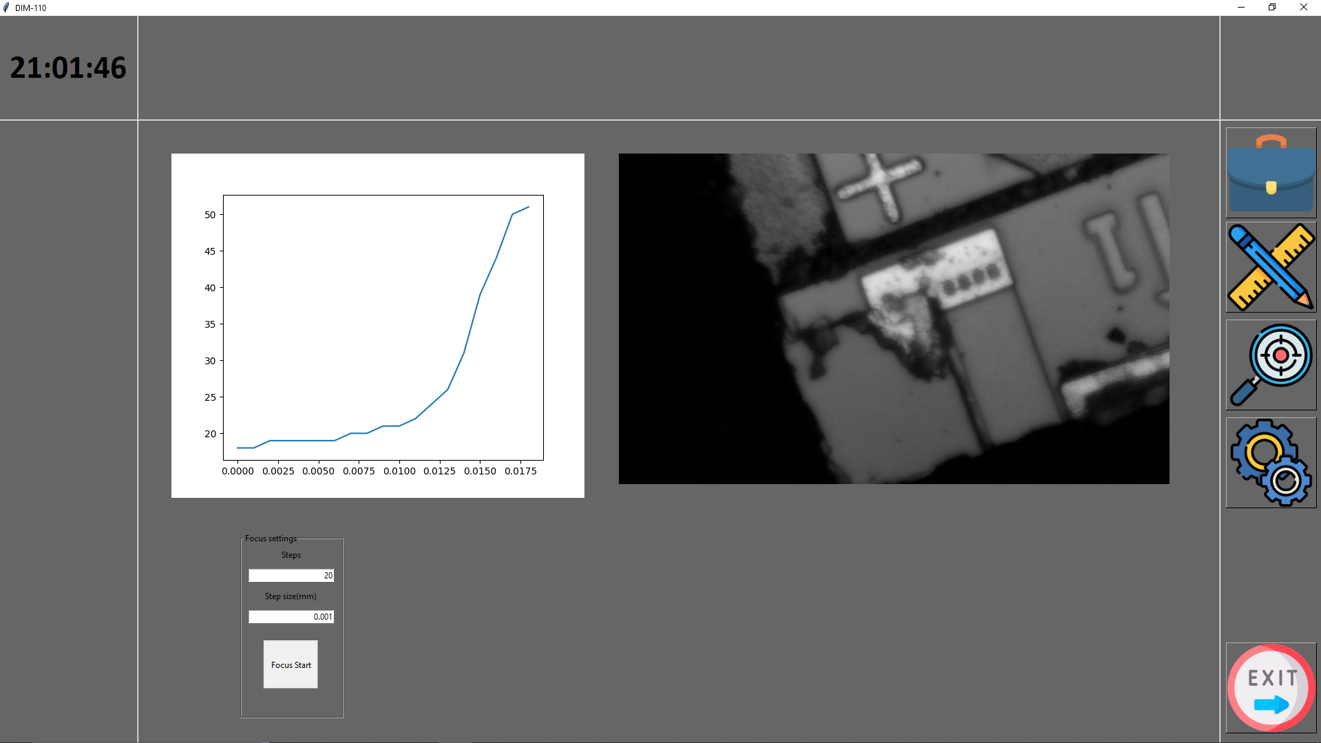
On the left bottom two additional parameter needed to be able to start the focus. First is how many steps we want and the second is how big shoud be each step. (for example: 20 step, 0.005 millimeter step size)
Recently I had the idea to use this focus contrast search for 3D scanning the surface of the integrated circuit (die). The idea is the same like what I used in focus method. Starts from the bottom, take a picture and with OpenCV laplacian function search the points which are in focus on the picture. You can see on the GIF I attached below, like how people eyes can see the parts which in focus on a picture, OpenCV can see the same and save these coordinates copied to an array. The Z axes steps 1 or 5 micron up every picture and the code saves the focused parts from each picture.
After it store into an array like a 3D array we can show it with some kind off 3D scatter diagramm, like you see below (the picture and the 3D model is mirrored, still have to fix it):
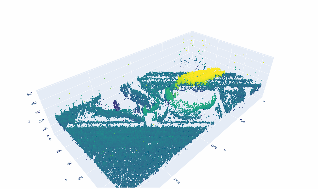
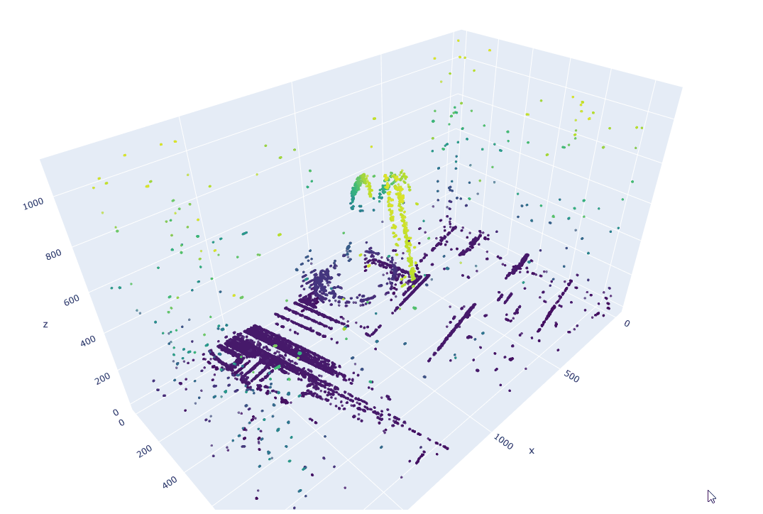
On the above model we can see a 3D height map from the DIE. The big thing is a broken bonding wire which left over when I openned the IC case. (the hight of that yelow bounding wire peace is 60 micrometer!)
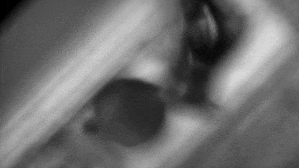
The below GIF we can see a still attached wire bounded connection which goes out to the case of the Integrated circuit.
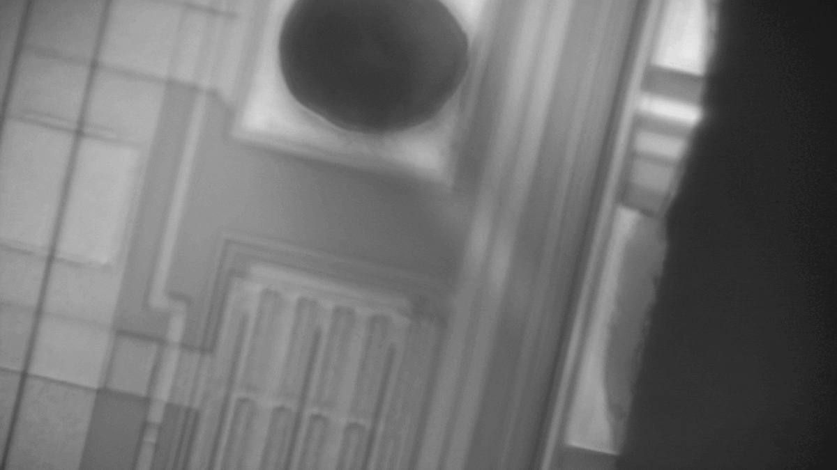
The map of the attached bonding wire. The wire connect to the square pad. There is quite a bit of noise in the map, but the shape and location can be seen on it:
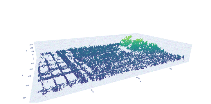
Next one is a broken Wafer die, which I broke during decapping, but thanks to this one peace on the edge bended up and made a perfect candidate for a 3D scan demo:
The map:
I am quite happy with the results, I have never seen anybody do this before.
Status of the microscope:
- UI interface comming together still have to make it not run serial. Make treading or task managment.
- Can auto focus on any point of the chuck
- Can scan like a snake and from thise pictures stich large maps together
- Rough 3D scan methode implemented, still have to put togehter with DIM-110 software.
- Can scan wavelenght and from that calculate reflectance on sample.
Discussions
Become a Hackaday.io Member
Create an account to leave a comment. Already have an account? Log In.