CPU architecture
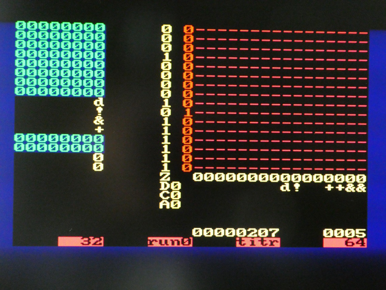
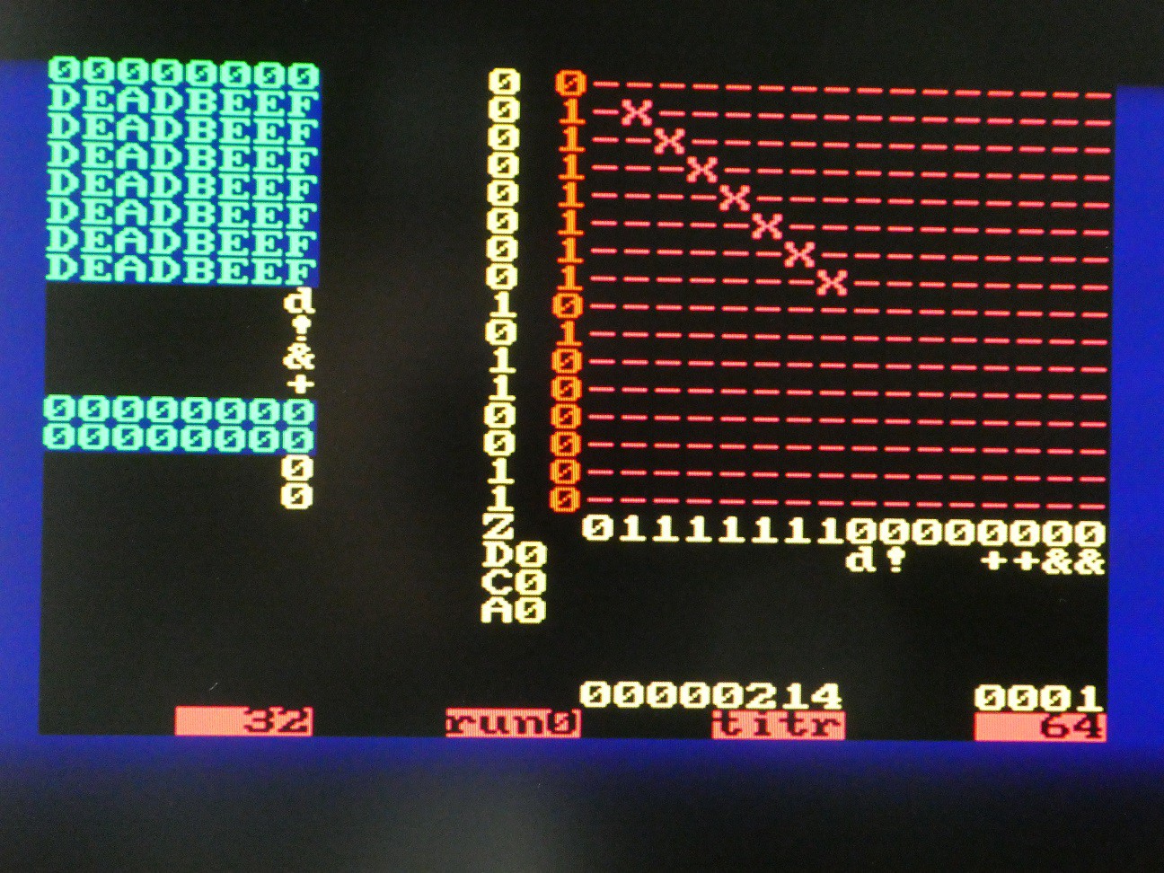
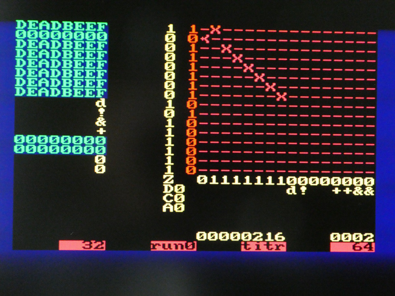
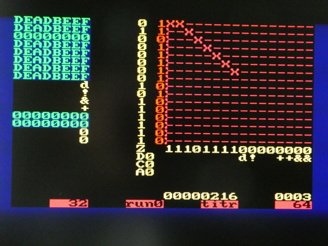
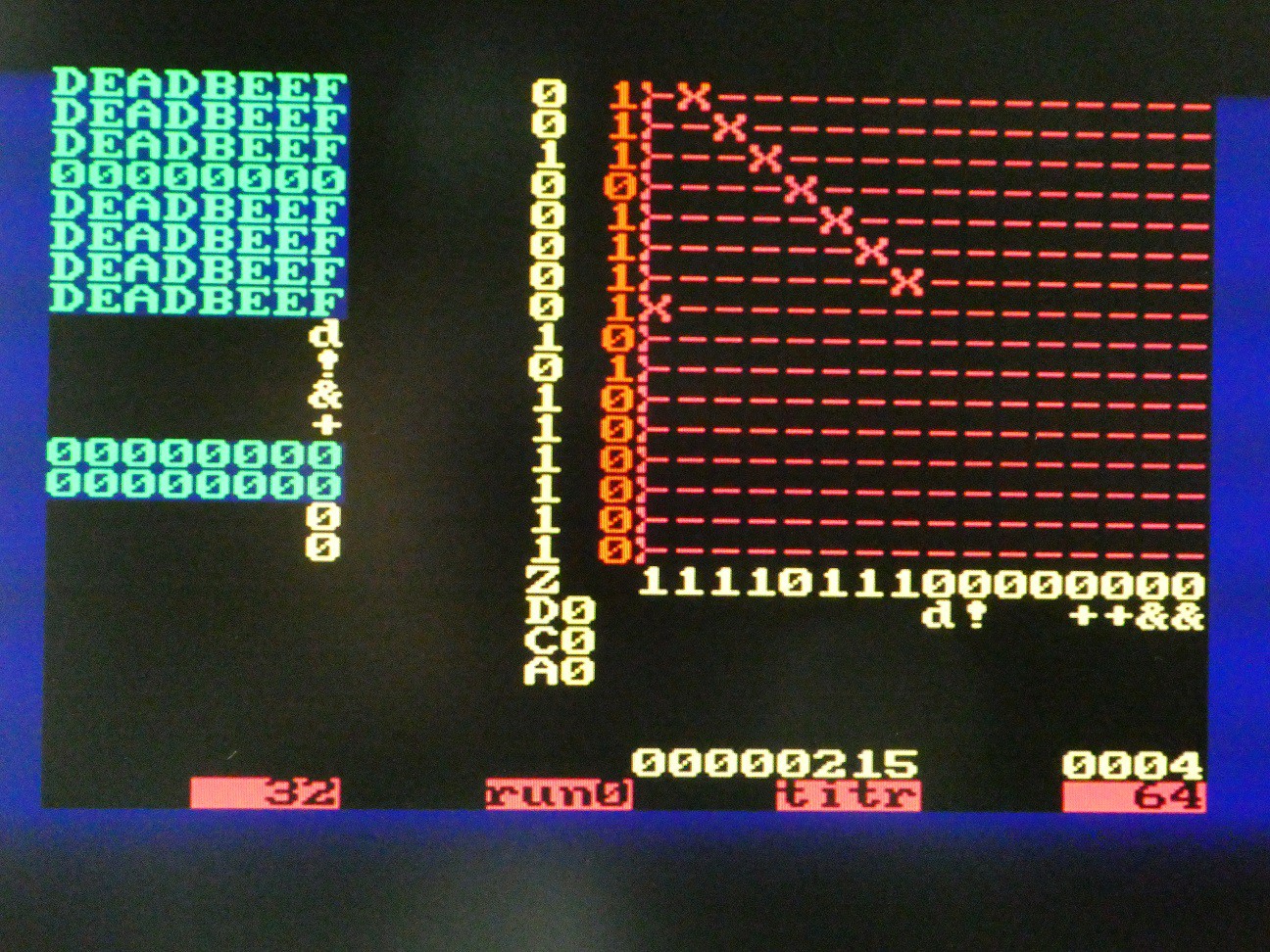
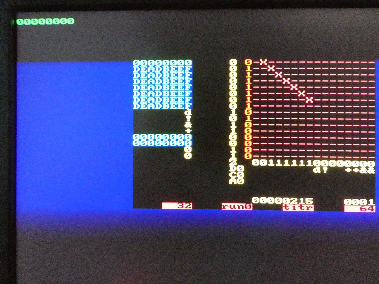
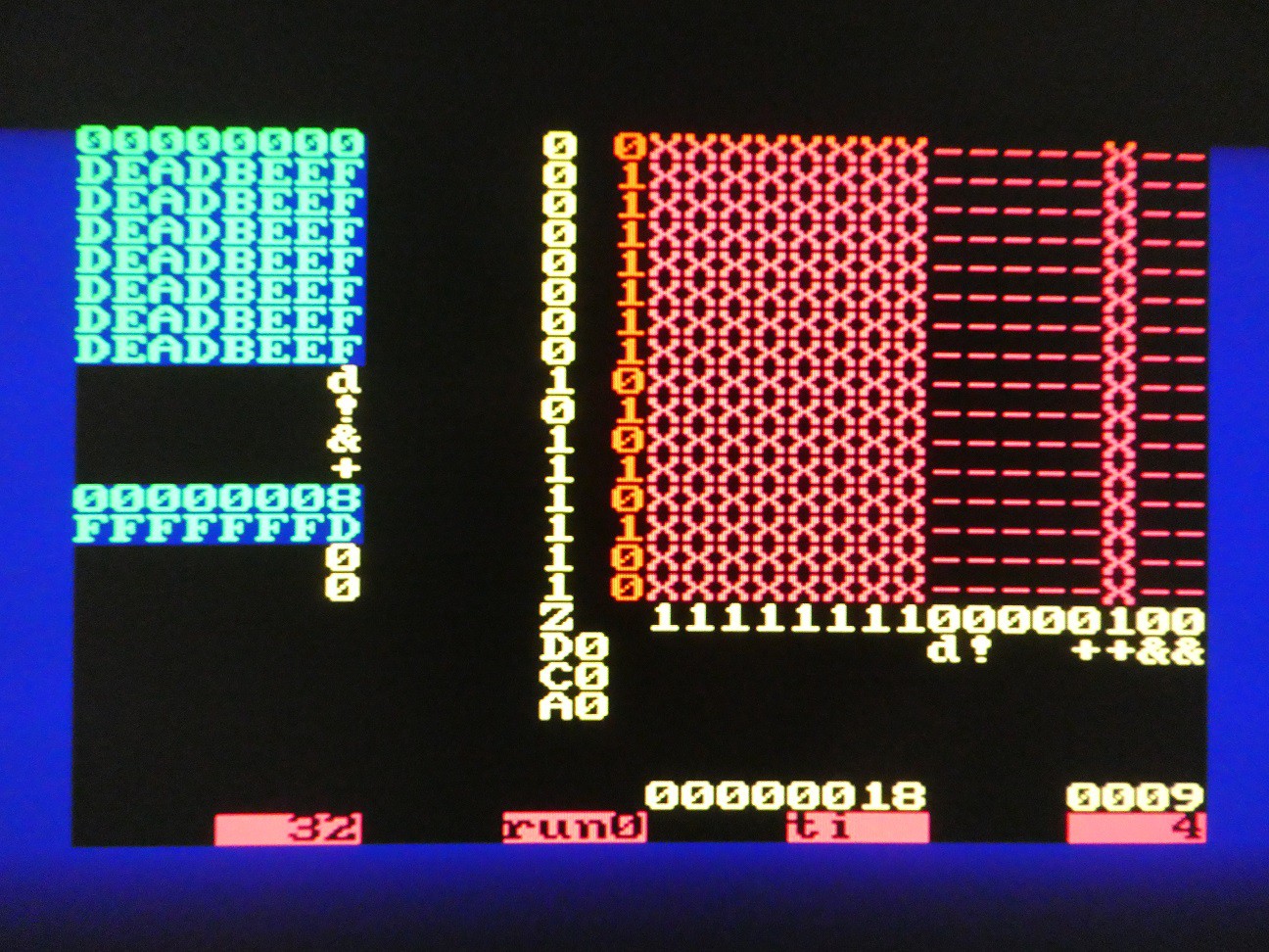
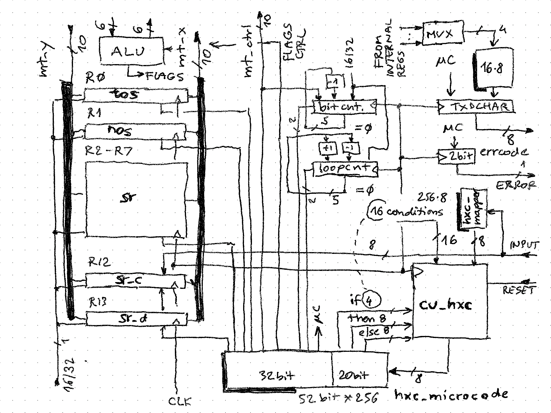
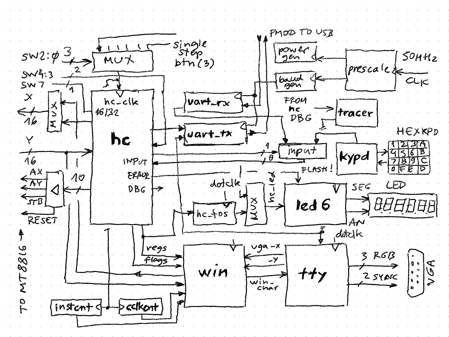
A simplified schematic of the CPU illustrates the main components:
- The switch matrix - the inputs (rows) are connected to the outputs of registers and outputs of processing elements, while outputs are inputs to registers and processing elements. Any number of switches can be on or off, and this is done under program control (microcode, or state machine). It is important to note that output column wires have "pull-down" - this means if no switch is on in that column, the output will be 0. This way, logical OR can be implemented on any number of inputs simply turning on multiple switches in a column (of course, an opposite implementation could generate a wired AND)
- Register stack. In simplest form, they are shift registers with common clock - at each clock time 1 bit is presented to their outputs (going into switch matrix) and 1 bit picked up on opposite side (from switch matrix). If the word length is n bits, after n cycles the value in register is unchanged.
- ALU operators. These are either simple logical gates (NOT, NAND, XOR etc. - note OR is not needed as it is "baked into design") or 1-bit state "machines". For example a full-adder requires a 1 bit carry flip-flop to keep the carry between each bits as they are added, or a delay flip-flop that allows implementing shift up/down operations. Both of these flip-flops can be set/reset/unchanged under program control, and their state examined for branching etc.
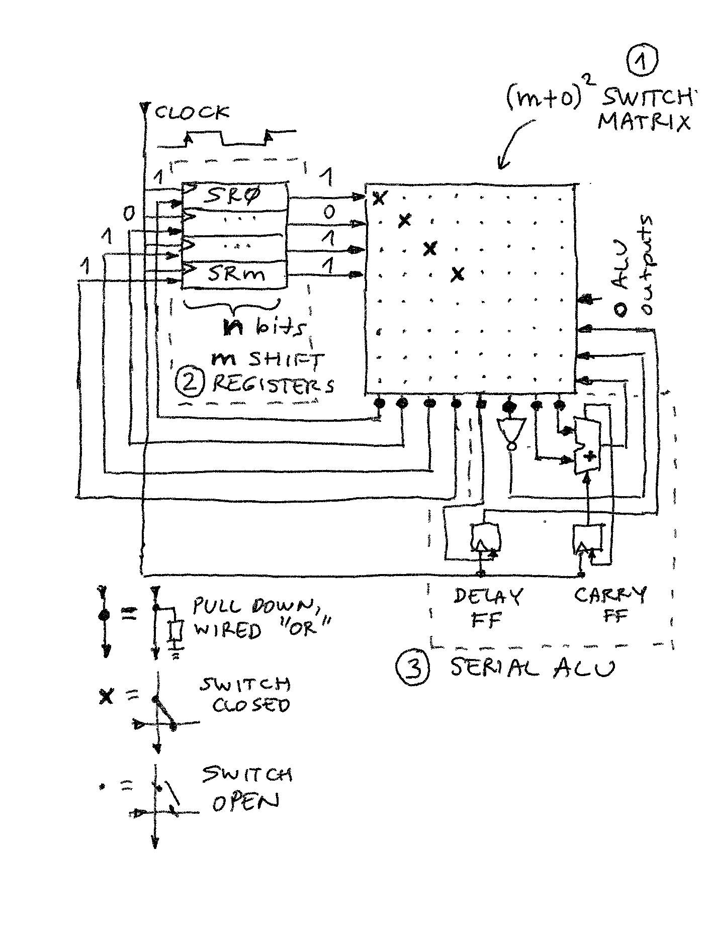
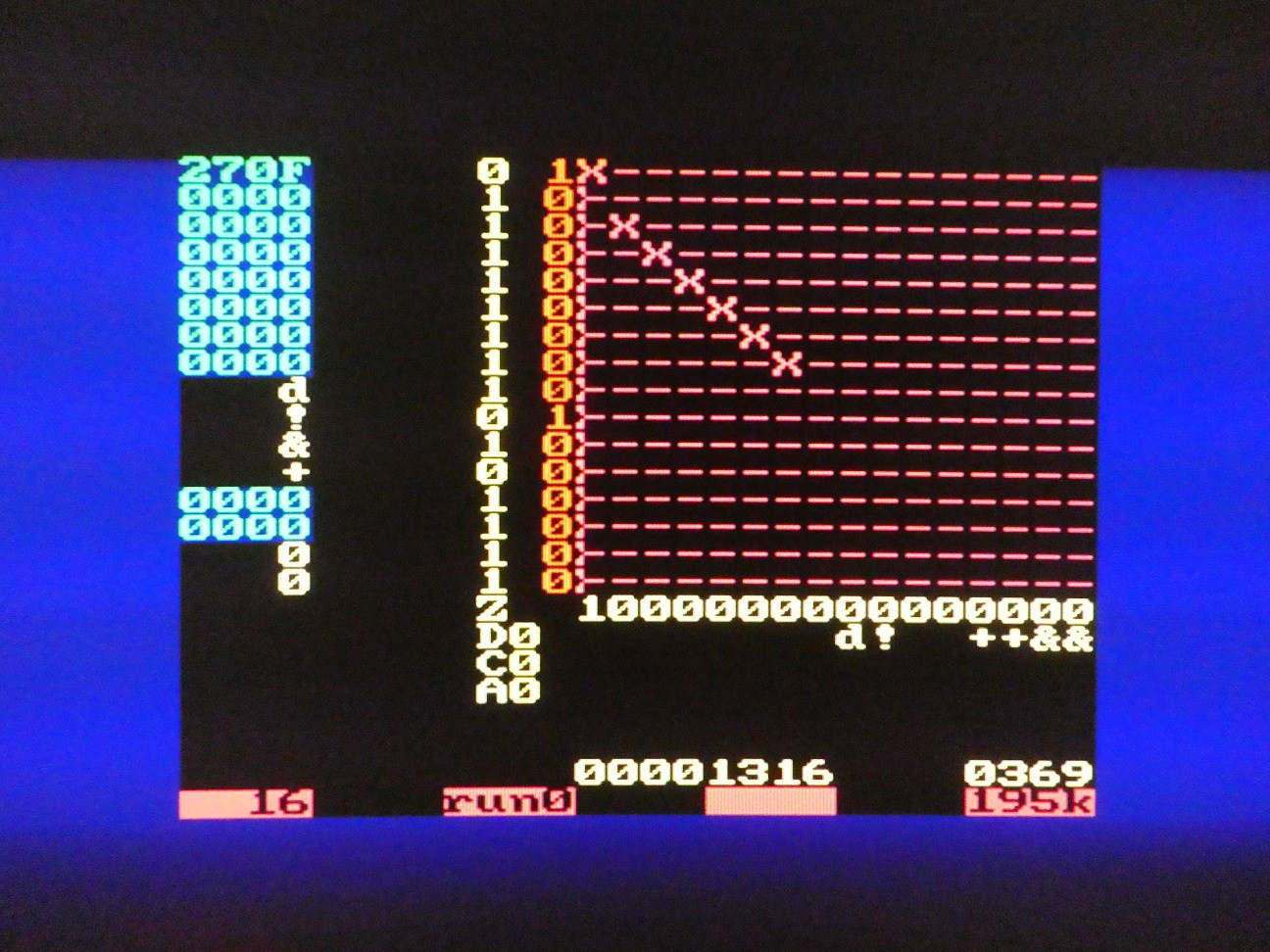
NOP operation is illustrated - all switches are OFF except the ones on the "register diagonal" - this means the "head" of each register is connected to its "tail" so after every n clock cycles nothing changes.
Move and logical operations
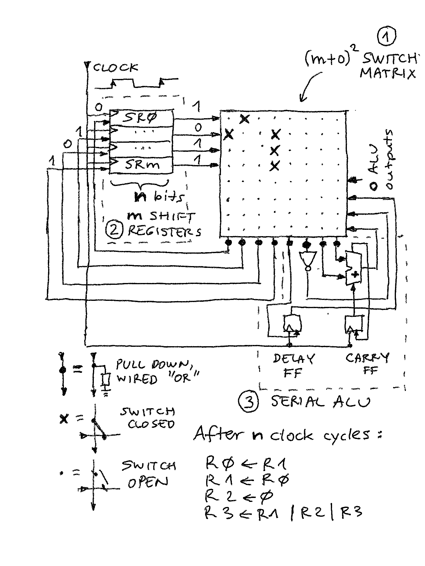
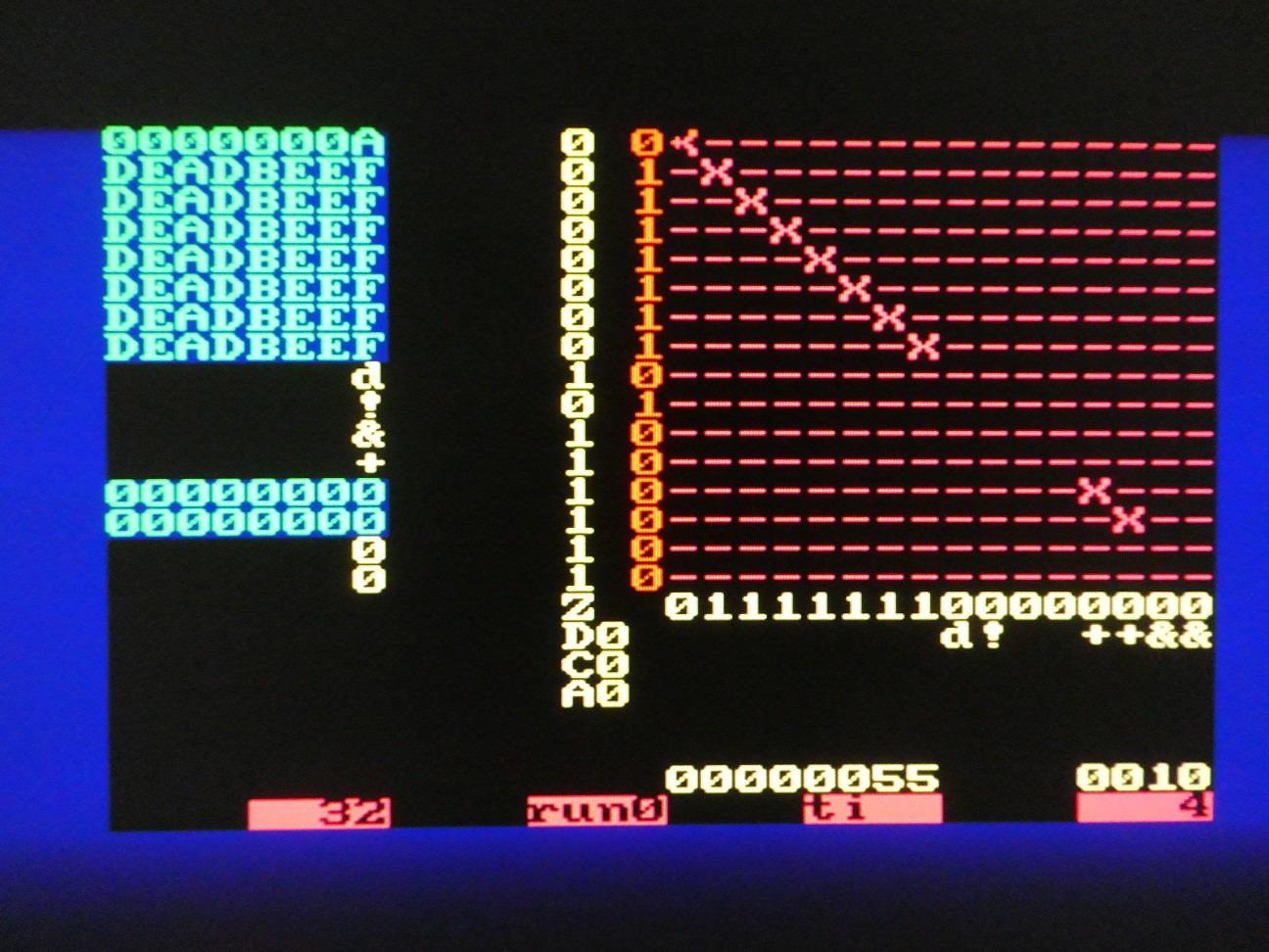
With switches on only in the "register quarter" top-left, many moves, loads, and logical operations are possible. It is best to read by columns:
- 0: connected to row 1, therefore R0 <= R1
- 1: connected to row 0, therefore R1 <= R0
- 2: not connected, pull-down will keep it at 0, so R2 <= 0
- 3: connected to multiple rows, 1 on each of them will pull the column up to 1 (wired OR), R3 <= R1 | R2 | R3
Note:
- 4 operations can be executed in n clock cycles
- exchanging registers possible without temp storage
- number of inputs and outputs is flexible (for example result of R1 | R2 | R3 could have been assigned to all 4 regs at once!) unlike standard 1, 2, 3 operation field instructions of most CPUs.
Arithmetic and logic operations
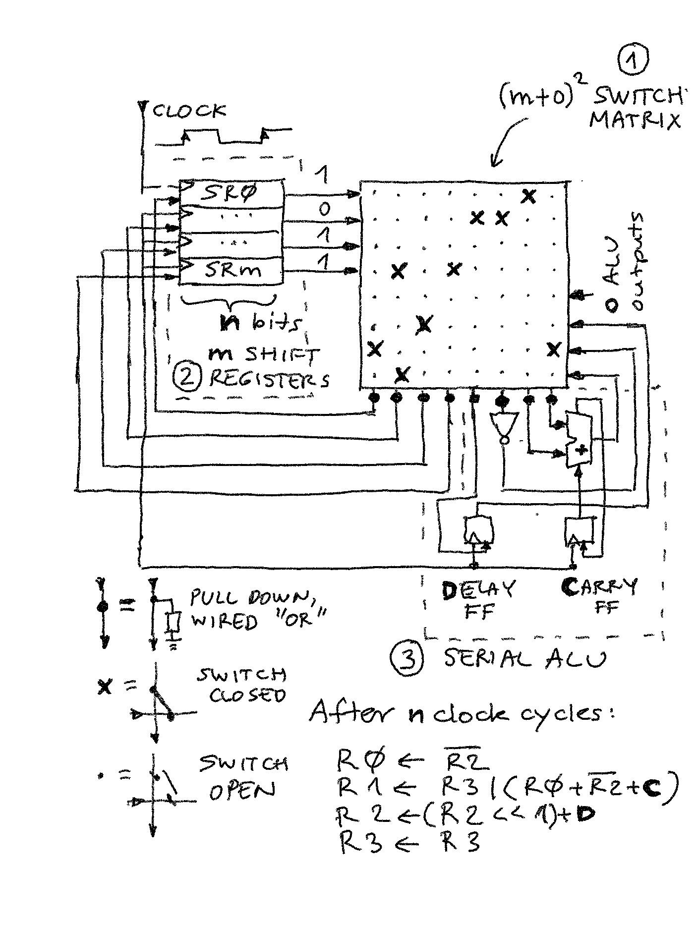
The connection matrix is more complex now. Register assignments are read column-wise 0 to 3:
- R0 is output of NOT
- R1 is OR between R3 and output of full adder
- R2 is output of delay flip-flop, so will be what went in there in cycle n-1
- R3 is connected to itself only (NOP)
The connections to ALU elements are read by columns 4 to 7:
- delay flip-flop input is R2
- NOT input is R2
- first input of adder is R0
- second input of adder is output of NOT
Combining these, we see the results of register updates on the pic. If the shift direction is LSB first, and C is set to 1 initially, R0 - R2 is executed. Of course, the result does not need be stored so a comparison operation can be executed along with copy, set etc.
Delay bit processing
Delay bit can be used to implement any number of shift and rotate operations. If R contains r7...r0, then:
- LSB shift after n cycles: r6 r5 r4 r3 r2 r1 r0 D ("logical shift left")
- MSB shift after n cycles: D r7 r6 r5 r4 r3 r2 r1 ("arithmetic shift right" if D is set to r7 initially, or "logical shift right" if set to 0 initially)
- Matrix can of course be reconfigured during the shift to inject D at any point so it can appear anywhere in the final register value
 zpekic


 spudfishScott