 zpekic
As noted in other logs, it was difficult to run the CPU at >2MHz or so, most likely due to R/L/C impedances and skewed signals from 6+ in wires from the PMODs to breadboard holding the 2 physical MT8816 ICs.
But what if the switch matrix was inside the FPGA, not outside, how fast could it run? To try that out, I developed a "virtual replacement" for the 16*16 switch matrix, and called it (very original!) MT16x16.
Replacing a true analog switch array with FPGA would be only possible using very fancy and expensive FPGA chips which have analog paths. Luckily, MT8816 in this design is used as a "wired or" not really analog, so it is possible to create 256 D-type flip-flops, each controlling an AND gate connected to a row input (X), and 16 of these OR'd together make up a column output (Y):
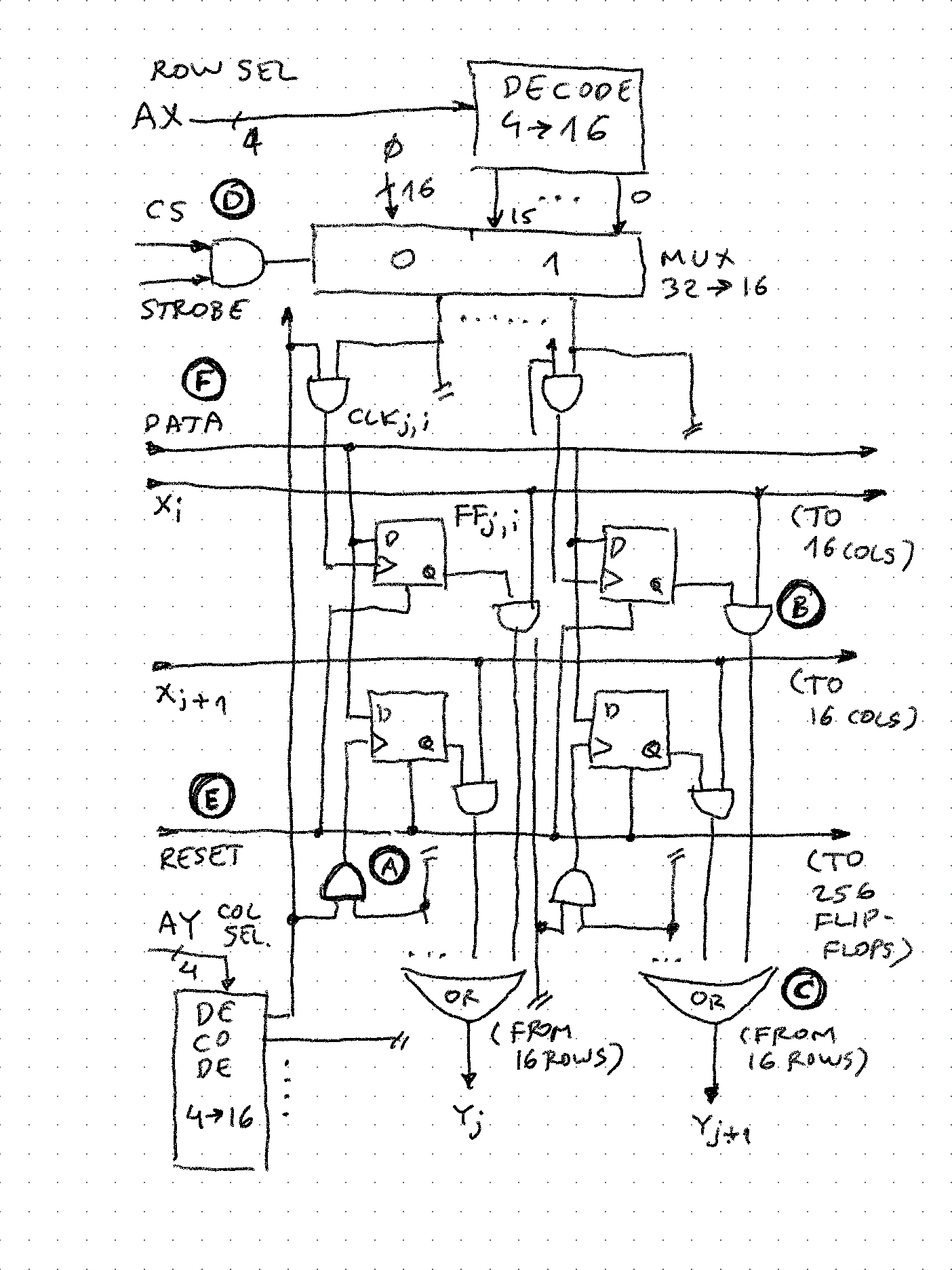
Noted on the schema above:
- (A) - the clock for each flip-flop is generated by 2 input AND that registers the coincidence of row and column selection. This way only at most 1 FF can take the DATA input (same as real MT8816)
- (B) - FF output (traditionally marked Q like in classic 7474) is used as an "enable" signal to AND with the input row X
- (C) - 16 outputs of AND gates (B) are then OR'd together to form output column Y. The "wired OR" becomes clear - if at least 1 FF in the column is "set" and its X input line is high, the output of column will be high.
- (D) - while column decode (AY) is always active, row decode is only active when CS (chip select) and STROBE signals are both high. Outside component drives these signals from microcode, but enables them only during 4-phase clock phase 1 (to insure right signal levels are propagated before clocking the FFs)
- (E) - reset signal is routed to 265 FFs - this is very bad design in FPGAs are routing resources are limited, but it worked. Outside component also drives reset signal from microcode and phased clock to prevent misfiring (microcode only used 2 bits to encode set, clear, reset all and nop - in hindsight this was a bad design decision because probably with 1 hot encoding (and just 2 bits more wide microcode word) the 4-phase clock would not be necessary.
- (F) - data input is also routed to all 256 FFs
In VHDL code, this 16*16 matrix is generated and interconnected using 2 generate loops. The column Y OR is pulled out of inner loop to make sure all ANDs are parallel and not stacked serially.
With external wires eliminated, CPU can be driven up to 25MHz clock frequency (microcode execution at 6.25MHz due to 4 phase clock). This means that an integer square root of 32-bit number takes typically 16305 to 94195 cycles which means 2.6 to 15ms.
CPU frequency is selected using switches 2..0 on the FPGA board. This gives 8 choices, the upper 4 of which select operation using internal matrix, and lower 4 with external (slower, but more fun!) MT8816 chips:
-- select the clock
with sw_clksel select mt_cnt <=
    ss_cnt    when "000",    -- single step
    freq_2048(9 downto 8) when "001",    -- 4Hz        -- EXTERNAL MT8816
    freq_2048(5 downto 4) when "010",    -- 64Hz        -- EXTERNAL MT8816
    freq_50M(5 downto 4) when "011",    -- 1.5625MHz     -- EXTERNAL MT8816
    freq_50M(4 downto 3) when "100",    -- 3.125MHz    -- INTERNAL MT16x16
    freq_50M(3 downto 2) when "101",    -- 6.25MHz    -- INTERNAL MT16x16
    freq_50M(2 downto 1) when "110",    -- 12.5MHz    -- INTERNAL MT16x16
    freq_50M(1 downto 0) when others;    -- 25MHz     -- INTERNAL MT16x16
Given that state of the matrix is reset and changed during the instruction execution (in other words, switch matrix state does not contain data to preserve from one operation to the next), it is possible to switch use of internal/external and back between instructions. Theoretically, it could be possible even to change the use while calculating an operation (because switch on/off commands are sent to both matrices regardless of which one is in use), but I haven't tried it and might fail due to glitches during such switch.
Discussions
Become a Hackaday.io Member
Create an account to leave a comment. Already have an account? Log In.