Close
0%
0%

World's first 32bit Homebrew CPU

Creating the world's first 32bit homebrew CPU using 74' series logic.

Similar projects worth following
There is a major CPU that is missing from the world. A 32bit homebrew CPU that implements a full and modern instruction set. The solution is to use 74' series logic chips and the RISC-V open source instruction set architecture. With a GNU toolchain already created for RISC-V it means we already have an assembler and compiler ready and waiting for our machine. So lets get rocking and create the ultimate in homebrew projects.

Browsing the web, I found a fascinating niche activity. People have built homebrew CPUs/computers using just basic logic chips. And they actually worked, they did real computation. These ranged from trivial 4bit machines, that barely did anything, up to impressive 8 bit machines that run a customized version of Mimix. One crazy guy in England has used several thousand transistors to create a machine that takes up half a room. They look cool, sound great fun to build and I want in on the action.

But what to do? Well there seems no point in just copying what others have done. The fun is in designing your own unique project and the journey taking it from idea to working machine. Well it seems worthwhile to tread new ground, do something not done before. As far as I can tell, there is no homebrew 32bit machine (I don't count an FPGA implementation). And certainly, none seem to implement a fully specified existing instruction set architecture (ISA). This is something that must change.

A bit of research later and I have found the perfect ISA. There is relatively new open source 32bit RISC architecture called RISC-V that has been designed by researchers at UC Berkeley. Being a RISC design, it is relatively small in the number and complexity of the instructions that need implementing. This is important as any 32bit design is already going to be a big project, so lets not make it impossible by going for something like the CISC of the 80386!

  • ALU - Shift

    Phil Wright11/10/2017 at 01:30 0 comments

    The most complex part of our ALU is handling the various shift operations. We need to handle shifting left and right as well as the logical and arithmetic variations. So the design is constructed in the following modular way.

    Our 32bit machine allows a shift distance of 0 to 31 places that means we have 5bits describing the shift distance. To implement this we need a single shifter for each of the 5bits. The first shifter looks at bit 0 and if set will output a value that is the input shifted one place left. The second shifter looks at bit 1 and shifts the output 2 places. Bit 3 causes a shift of 4 places, bit 4 shifts 8 places and finally the last shifter moves 16 places left. By flowing the output of the first shifter as the input to the second, and so forth, the final result is shifted the correct distance.

    By default we shift left (to higher bit positions) but we also need to handle a right shift as well. We definitely want to avoid creating another 5 level shifter for handling right shifting. Instead, we reverse the input bits before and then again after the shifter.

    The SRA and SRAI operations are arithmetic right shift operations, meaning the most significant bit is replicated to the right as the shift occurs. This is useful if you want to shift a negative number and retain it as still being negative afterwards. To support this we use some extra logic for deciding if zero or one is used when filling blank bits during shifting.

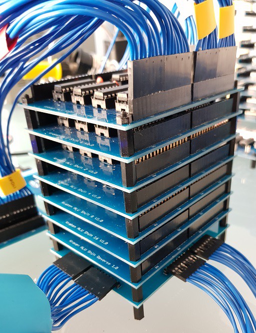
    Finally we need to use a tristate buffer so that the entire output can be turned off when the ALU wants to ignore the shift output. Our final design consist of the following boards from top to bottom:-

    • Reverse
    • Shift 1
    • Shift 2
    • Shift 4
    • Shift 8
    • Shift 16
    • Reverse
    • Buffer

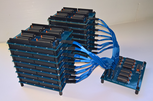
    The final tower looks like this:-

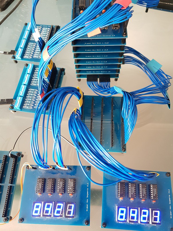
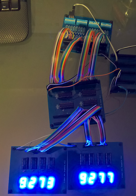
    To test the stack we need a 32bit input, 10 control lines and then be able to examine the 32bit output. Like this:-


    Implementing a shift board needs 8 x 74HC241 and the reverse board also uses 8 x '241. We can also make use of the '241 for the buffer board. So I ended up with a total of 56 of them in the stack. 

  • ALU - Less

    Phil Wright11/04/2017 at 03:50 0 comments

    The third section of the ALU is the ability to compare two numbers and output either 0 or 1 depending on if the first value is less than the second. It has the extra complication of allowing comparison of signed and unsigned numbers.

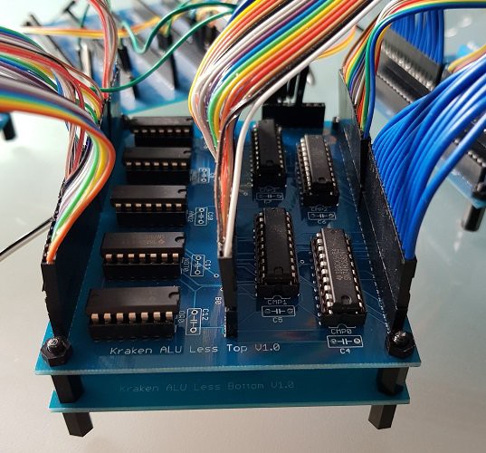
    Implementation is simple enough as it is just a cut down version of the full compare board I have already created elsewhere.  It needs two boards stacked in the usual vertical fashion using long female headers. It uses 4 x 76HC682 8bit comparators and then a little gate logic to determine the result. Unfortunately there is a just a little too much logic to fit on a single board.


  • Immediate Values

    Phil Wright10/22/2017 at 23:20 0 comments

    Many of the RISC-V instructions encode immediate values within the instruction. Converting these encoded values into actual 32 bit values is dependent on the instruction type. There are 6 instruction formats but only 5 contain an immediate value.

    Our design spans two boards and takes as input the full 32 bit instruction and control lines indicating the instruction type. (The type is discovered by the decoder elsewhere). The logic is simple enough but not so simple that I avoided a mistake the first time around. Hence the boards are marked as V1.1, as shown below.

  • ALU - Logical Operations

    Phil Wright10/22/2017 at 23:09 0 comments

    RISC-V specifies three different logical operations, AND, OR and XOR.

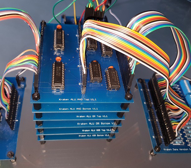
    Each operation needs 8 chips for the actual operation, such as using the 74HC08 for the logical AND of the 32bit A and B inputs. Plus, another 4 x 74HC241 for the output buffer. All ALU operations are output to the same bus and so each operation needs an output buffer that ensures only one result is output at a time. Unfortunately, 12 IC's is too many to squeeze onto the 100mm x 80mm boards that I use. So we are forced into splitting it over two boards, one that does the lower 16bits and the other does the upper 16 bits.

    We end up with a stack of 6 boards where long female headers providing the A and B inputs and the output result traversing the entire stack. Control lines determine which operation, if any, is performed.

  • ALU - Add and Subtract

    Phil Wright08/08/2017 at 00:01 0 comments

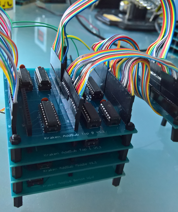
    The ALU for our CPU needs to perform several types of operation. The first of these is the ability to add or subtract two 32-bit numbers. To implement this I have built a stack of four boards that combine together to give the output.

    Adding two numbers is simple, we just use 4 x 74283 and chain the carry output of one to the carry input of the next in sequence. This has been implemented as the 'AddSub Middle' board below.

    Implementing the subtraction operation requires a bit of extra work as we need to apply 2's compliment to the second of the two inputs. 2's compliment is the method used to invert the sign of a value. Converting a positive number like 5 into the negative version -5.

    This approach avoids the need to implement a separate subtraction circuit and instead allows reuse of the existing addition circuit. For example, 10 - 5 can be implemented as 10 + (-5).

    2's compliment is very simple, you just invert all the bits and then add 1. The purpose of the top two boards is to invert all 32-bits of the second input when the control line indicates a subtraction is needed. Adding the extra 1 can be done in the middle layer by providing a initial carry in value to the first adder.

    Finally, the bottom board is used to buffer the output, as only sometimes will the ALU want to perform an add/sub operation. All outputs from the different parts of the ALU are connected to the same output bus and so only the appropriate ALU section should put its output on the bus.

  • Comparator Complete

    Phil Wright07/19/2017 at 00:43 0 comments

    I have been delayed recently by a bad batch of 16 pin long female headers. They arrived from China but were sub-standard, inserting a connector at the top caused some of the bottom pins to be pushed out. They simply didn't work. But a new batch has arrived that works and we are back in business again.

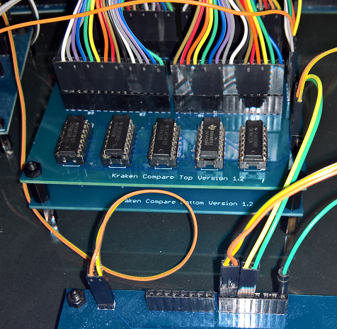
    The 32bit comparator is split into a top and bottom board because there is not enough space to fit it all on a single 100mm x 80mm board. The top board begins by using 4 x 74682 chips to compare each of the 4 bytes from the first and second values.

    Only if all four compares are equal is the 32bit compare also an equal. Discovering if the first value is less than the second is more complicated because there are several combinations that result in the less than result: -

    • First byte is less than and the top three higher bytes are equal
    • Second byte is less than and the top two bytes are equal
    • Third byte is less than and the top byte is equal\
    • Fourth byte is less than

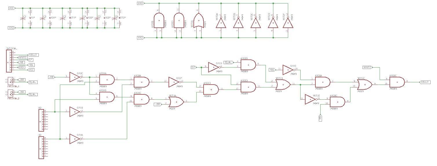
    Adding the logic for calculating the equal and less than outputs of the top board results in the following logic diagram: -


    The bottom board takes the basic output of the top board and applies some extra logic. One of the control inputs is called NEG and is used to negate the output. For example, the branch if equal (BEQ) and branch if not equal (BNE) instructions only differ by setting this NEG control line. Another control line is called UNS and determines if the comparison should be signed or unsigned (BLTU, BGEU instructions). Finally a RES line is used to decide if a result should ever be output. This allows the output to be forced to zero. This is needed because the output of the board will be used as the control line input for a MUX elsewhere. We want to force the value to zero unless we are processing a branch instruction.

    Here is the logic for the bottom board: -Testing shows that the logic is correct and the boards work as required. Although each board only worked on the third attempt at debugging the logic.

    The comparator is going to be one of the slowest paths in the whole design. If you look at the worst path through both boards then it has 18 gates to get through. Yikes, good job I am not designing for speed!

  • 32bit Comparison

    Phil Wright07/02/2017 at 07:53 0 comments

    My processor needs the ability to compare 2 x 32bit values and output a simple true or false. In addition to the values it has a few control lines that indicate the operation (=, <, >=), if the comparison should be inverted and if the comparison is between signed or unsigned values.

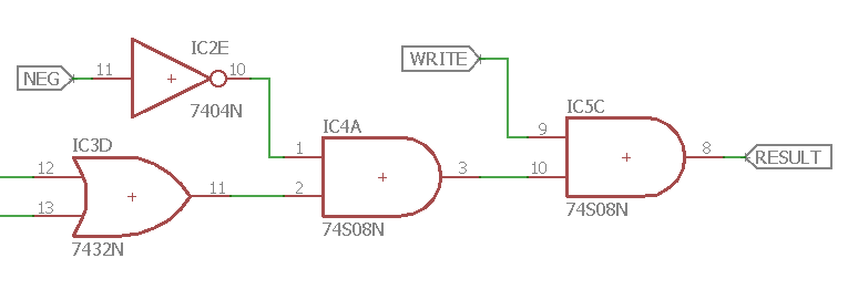
    The design is split between a top board that does the basic comparison assuming the values are unsigned. Then the bottom boards take into account the negation and unsigned requirements. Doing a test on this bottom board shows it giving incorrect outputs for when the negation is applied. So I check the circuit design so I could start debugging. Well it didn't take long to find the issue. Here is the last stage of the circuit where it takes negation into account...

    Well that is garbage. Instead of negating the output if the NEG input is true, it simply always outputs zero. So a quick fix solves the problem thus...

    Amazingly the cost of boards from PCB Way has gotten even cheaper. Now just $5 for ten boards, so the fix is a pretty cheap one to resolve.

  • Instruction decoder

    Phil Wright04/05/2017 at 03:51 6 comments

    Instruction decoding is one of the simpler parts of the system. For example, all the branch instructions can be identified using the same 7 bits of the incoming instruction value:-

    All branches have the same '1100011' pattern at positions [0-6]. So I only need a single decoder board that compares and matches this 7 bit sequence in order to generate the correct control lines for the rest of the CPU. The actual comparison of registers rs1 and rs2 is performed by a separate comparison board. This comparison board takes as input the 3 bits at positions [21-14] that uniquely identity the actual branch operation. So '000' will mean BEQ and '001' BNE and so forth.

    This same approach works for other major groups as well. All the ALU operations that take an immediate value have the same '0010011' pattern. The ALU operations that take two registers have the '0110011' pattern. In both cases the ALU implementation will perform the correct function by using the function code that is part of the instruction format and passed directly to the ALU.

    By grouping this way we only need a decoder board for each instruction group that we need to support. As I am only implementing 37 instructions it works out I will need 9 decoder boards.

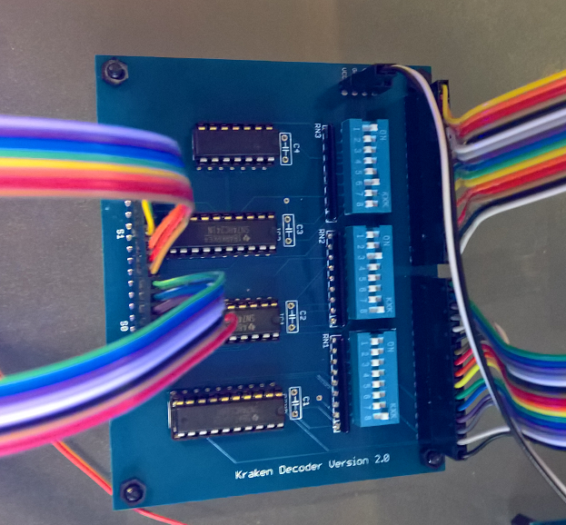
    A single board looks like this:-

    At the bottom right is an 8-DIP switch that is used to match against the incoming first 7 bits. This means the left most switch on this DIP package is not connected and ignored, but it is easier to order and use 8-DIP packages than try to find ones that support exactly 7.

    Above that are two more DIP packages that are used to define the 16 control output signals. I am assuming that my final design will not have more than 16 different MUX or other boards that need control lines!

    By making the board completely configurable I have the flexibility to implement the rest of the CPU in multiple ways and to change the design if needed. Like my other boards these can be stacked vertically because I am using long female headers for the instruction input, control line outputs and the power connection. So I anticipate a final setup with 9 of these high.

    I use a 74HC688 for the bit pattern comparison, 2 x 74HC241 output drivers for the 16 control lines and an 74HC04 to invert the output of the '688 for use with the output drivers.

  • Let it fly!

    Phil Wright03/20/2017 at 22:40 3 comments

    It took a whole weekend but finally the register file is complete. I took a delivery of new boards last week and the first to be built is the register control board. This is used to drive the 16 individual registers. Once finished it looks quite impressive...

    The control board takes three 4-bit values. The register to output on port A, the register to output on port B and the register to be written to. Our control board has three output headers that are 16 lines wide. So register zero takes bit 0 from each of the three headers as its input. Register one takes bit 1 from all three headers and so forth. This results in the monster wiring loom shown above. I had to make it all by hand using DuPont connectors, a crimper and some heat shrink tubing.

    It would have gone much faster except for some errors that took a long time to notice. Each of the two register stacks had misconnected pins in the middle of the stacks. When connecting them together it can be tricky getting all the 100 long headers to match up. Well I hadn't noticed a couple that had missed on insertion and were not connected. Compounding this I found that one of the ribbon cables I was using to make a test connection had two of the wires transposed. Luckily it was a rainbow coloured cable so I eventually noticed that red and blue lines were in the opposite order at the other end of the cable. Otherwise I would still be scratching my head!

  • Program Counter

    Phil Wright03/14/2017 at 22:18 3 comments

    The program counter module is split between two different boards because there are too many IC's to fit on a single 100mm x 80mm sized board. The top board provides storage by using 4 x 74HC574 IC's that each store 8 bits. Every clock cycle the storage is updated with the incoming 32-bit address. Because our CPU design is single cycle the PC needs updating every cycle. Hence there is no need for a control line that determines if the PC needs updating during the next tick.

    The current value is constantly output to a long header that is connected to the bottom board. This uses 8 x 74HC283 IC's to perform an add of the constant value 4. Because we are implementing the RV32E specification we know it does not need to support the condensed instructions, therefore all instructions are aligned on a 4-byte boundary. Moving to the next instruction always involves adding 4 to the current value. The CPU design will include multiplexors that determine how the input is provided to the PC. It could be the result of adding 4 but it could be the result of a conditional branch or the destination of a jump.

View all 23 project logs

Enjoy this project?

Share

Discussions

shahzebkayani wrote 02/16/2020 at 13:36 point

Hey there,
I want to do this as my undergrad's final year project.Can you help me out?

  Are you sure? yes | no

pentakillmaybe wrote 12/31/2019 at 09:04 point

Can you run Windows XP on this?

  Are you sure? yes | no

ATmel91 wrote 02/16/2020 at 20:34 point

no, you would need to run this at GHz of speed, this can probably only handle 100MHz~~ max due to the TTL chips limiting switching frequency.

  Are you sure? yes | no

enriquemesa8080 wrote 11/27/2018 at 23:13 point

Very good. I want to design my own CPU, at 8 bits scale. 8 bits scale sounds great for me. Currently i am looking for ways to build the registers. I plan to build the 8 bits register and adds a clock to count down the instruction counter or Program Counter, or Instruction Pointer (PC) (iP): This is the best thing i can do.

  Are you sure? yes | no

JDat wrote 02/25/2018 at 09:34 point

Hmm. You made first 32 bit homebrew CPU...

What about this? http://www.6502.org/users/dieter/trex/trex.htm

  Are you sure? yes | no

Phil Wright wrote 02/25/2018 at 22:32 point

Thanks for the link. I had not found this project when I did my google searching for 32bit homebrew machines. It looks like they never finished the project and it is now abandoned. Of course, I have not finished mine either.

  Are you sure? yes | no

agp.cooper wrote 11/30/2016 at 13:46 point

Hi Phil,

In "Register File Deux" you said "Based on the feedback I have come up with another design that brings the number down to 138 IC's and 18 PCB's. Quite the saving!"

Would you like to share your design/schematic? I would be very interested in having a look. I am particularly interested in your approach to the timing and instruction decoder.

----

I have used Eagle CAD but unless you pay more than $1k you are limited to 160mm x 100mm (=$169), which is in my mind is too small for a 32 bit CPU sub-board.

I use EasyEDA which is free web based PCB design tool. You can import and export your work (but it is not that faithful). The quote/manufacture is dead simple and pretty cheap (similar to the prices you mention). The main advantage is that there is practically no size limitations. Having said that it can be slow and auto-routing usually need to be manually edited (for large boards).

---

Something you should consider early is the connection/bus standard between the boards. Having a common bus standard will speed up PCB design significantly. It will also dictate the minimum PCB board width.

---

For 100+ TTL chips you will need a proper power supply. I spent a lot of time debugging my first CPU only to realise (after much frustration) that the power supply was not up to task.

---

You will need to think about your method for testing each board and the stack of boards as they are connected. I used an Arduino but you will probably need to use a Mega for the extra IO pins. I can safely say that if you expect the assemble the boards into a full CPU and expect it to work first time you will be disappointed. The game is really about minimising the number of concurrent errors (i.e. debugging a board with one error is much easier than debugging a board with multiple errors) and reworks (i.e. a new PCB).

---

Unfortunately, building a CPU also requires designing the user interface and operating system. How else are you going to test/demonstrate your CPU when finished? A front panel is okay for my simple CPUs but the more powerful CPU that you are planning will need something better. A serial terminal perhaps? You can cheat here and use a USB to serial converter and use your PC as a terminal (keyboard and display).

----

Anyway, the above are just suggestions and/or ideas, regards AlanX

  Are you sure? yes | no

Phil Wright wrote 11/30/2016 at 21:57 point

Hi

Your make some very good points, if you read the previous 'Register File' entry I outline a few more details. I will be building from 100mm x 80mm boards and so can use the free Eagle software. That means I end up with quite a few boards that need interconnects but that is fine by me. I am not looking to make the fastest CPU or the prettiest.

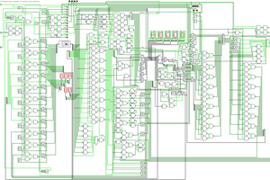
I am not designing it all in one go and then building, instead I am designing and building a section at a time in a modular way. I have an overall block diagram that you can see in the project images but the rest I design as I go. Not the most efficient way to go but as a hobby it is fun which is the main objective.

Testing will be done using a simple Arduino and using shift/latch IC's to go from serial to parallel to generate 32 bit values.

I am a professional programmer so the software side is easier for me than the hardware. I can use the existing open source GNU RISC-V tool chain to generate machine code from either assembly or C. I suspect I will write my own little OS for the fun of it. Maybe even my own assembler and C compiler and so make it self hosting. Time will tell!

  Are you sure? yes | no

agp.cooper wrote 12/01/2016 at 04:41 point

Hi Phil,

No problems.

If you are staying with the free version of Eagle and the 100mm x 80mm PCB limit, and don't mind lots of boards; You may want to consider strip-board construction. I used it for my Weird CPU (https://hackaday.io/project/12879-weird-cpu). I used DIYLC (free) for the design work.

The main advantages are:

1) its cheap.

2) it can be rewired if a mistake is made.

The main disadvantages are:

1) manual routing.

2) lots of wire links (I hate the wire links!).

3) limited bus width (~41 strips).

But if you are not using a bus standard then the limit bus width is not much of an issue.

Even though I now use EasyEDA, I still use strip-board for smaller one off support projects.

Regards AlanX

  Are you sure? yes | no

vasili111 wrote 03/21/2017 at 04:09 point

I think it is better to adap NetBSD for your CPU rather than making your OS from scratch. NetBSD was designed to be easy to port to other platforms.

  Are you sure? yes | no

Ingo M. wrote 11/28/2016 at 17:34 point

This is an awesome and very ambitious project! We really need such projects (and Open-V and the like) to ignite the Open Hardware movement. I intend to build the same CPU for myself when the first runs have been successful. I am amazed there have been no comments so far.

Good luck! 

  Are you sure? yes | no

Similar Projects

Does this project spark your interest?

Become a member to follow this project and never miss any updates