 Yago
YagoSo this is the progress in the soldering of the incompleted addressing board:
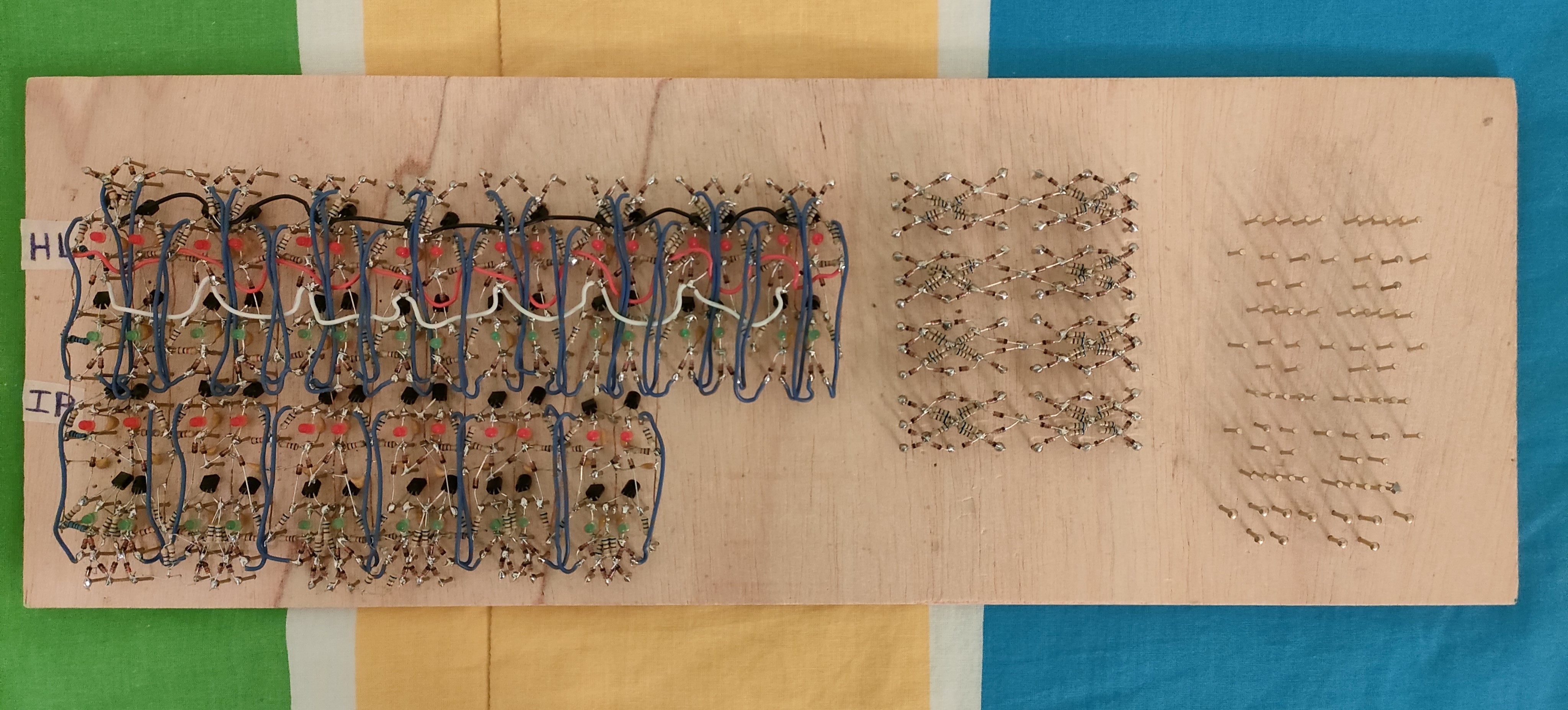
The upper row of circuits (the upper row of leds and such) is the HL (memory address) register, the lower row is the IP (instruction pointer) register. The square in the middle right is the multiplexer, which contains AND & OR gates, and finally, the incompleted circuit on the right are the output inverters. Terminal blocks will be placed on the top of the board to allow connection to other boards. In theory, there will be 4 other boards like this one.
Discussions
Become a Hackaday.io Member
Create an account to leave a comment. Already have an account? Log In.