 Christoph
Wolfgang designed his PCB in PCBExpress (I think), so I recreated his layout in KiCad. This was the result:
This was pretty small already, but was quite inconvenient for a couple of reasons:
- The power supply didn't have a connector, it was done through two soldered wires. That's not a problem per se, but the signal output is done through an SMA jack. It was only partially "pluggable".
- Without an RF shield, touching the probe changes its output. That is indeed bad.
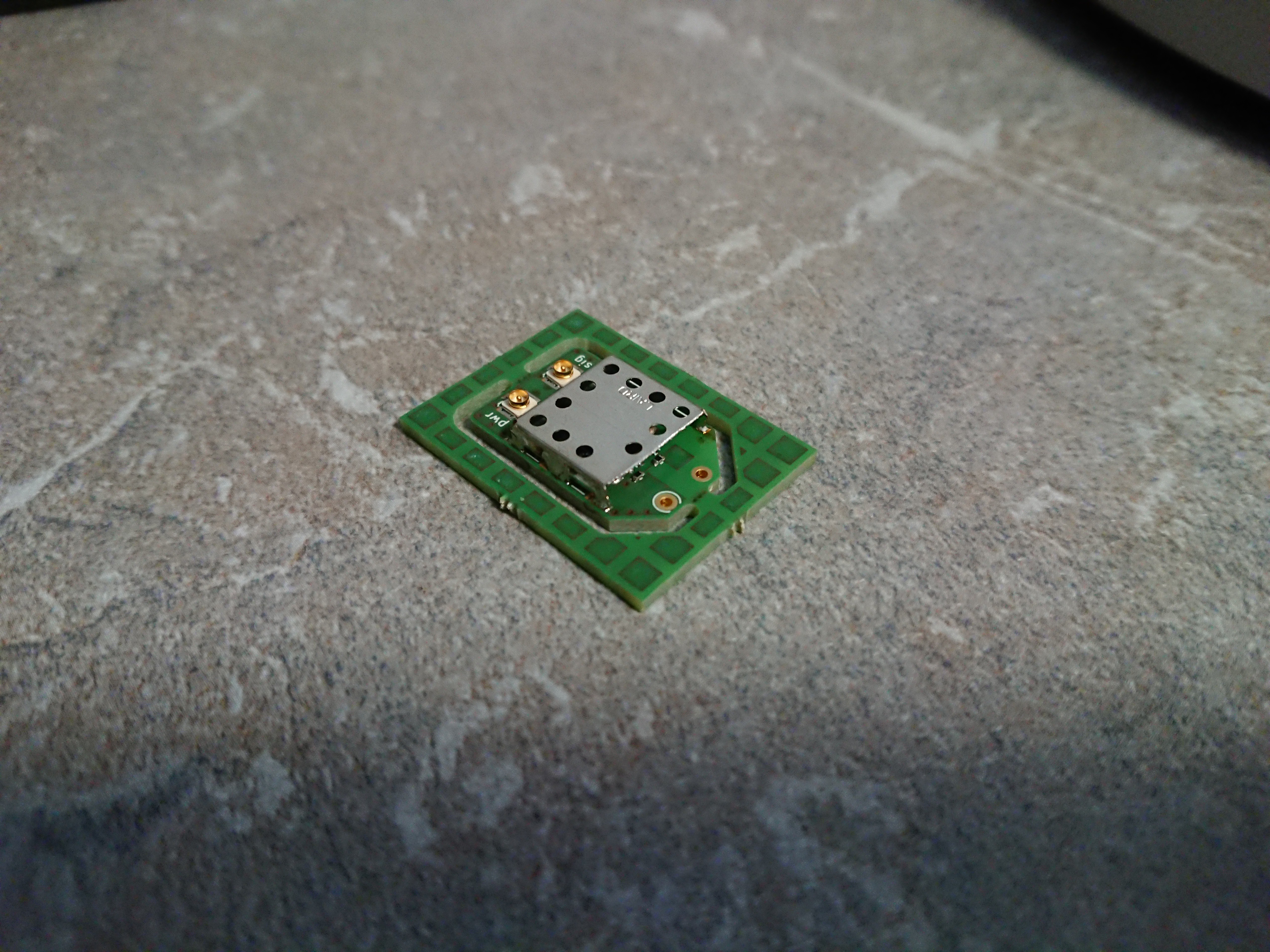
I sent it to Wolfgang anyway, and it performed well. The next step was to improve the design a bit towards a tool that can be handled well, and that can be solderen into a circuit (for when lead inductance really counts). The SMA was swapped for a u.Fl, and so was the power supply input. Adding an RF shield wasn't so easy because the common, small, off-the-shelf parts all have four walls. I picked a small one that looked easy to modify, and came up with this:
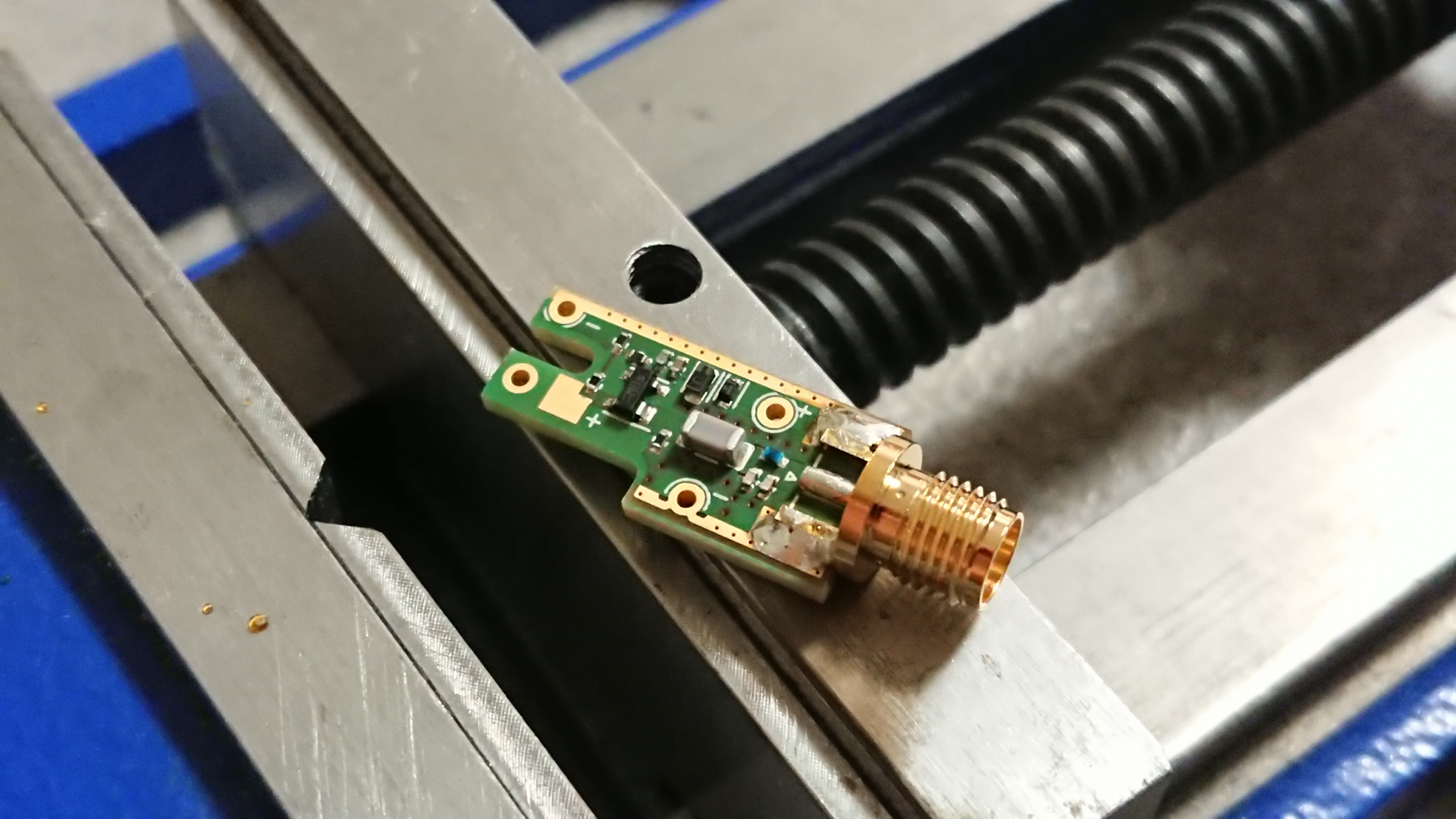
This is the probe characterized on Wolfgang's page:
https://electronicprojectsforfun.wordpress.com/solder-in-probes/
Next log will be about assembly and will also contain a link to a repo with layout files and all that.
Discussions
Become a Hackaday.io Member
Create an account to leave a comment. Already have an account? Log In.
Nice!!!!!!
Are you sure? yes | no