 Leonardo Ward
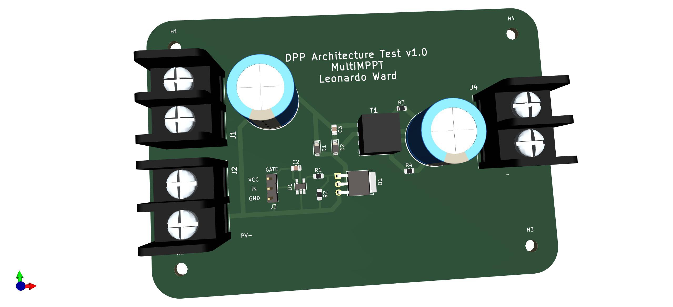
This PCB was designed to test the DPP architecture used in MPPT designs. The software used to designed the PCB is Kicad 6.
To get the PCB design (e.g. schematic, PCB, gerber files) check the following repository.
The tests performed with this PCB will contribute to develop the project MultiMPPT, that is a low cost high efficiency MPPT with multiple inputs.
Hardware Design
The following image contains the schematic of the PCB:
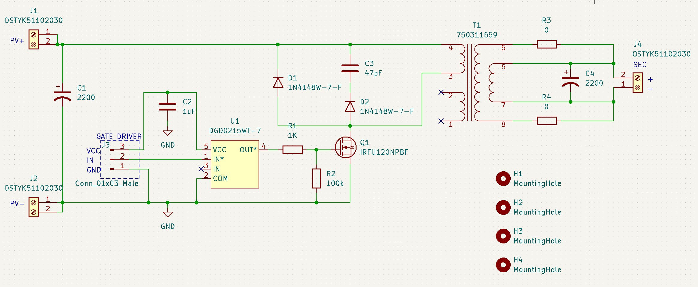
Where:
- J1, J2 and J3 are used to connect the solar panel and connect to other components inside the MPPT (during the tests).
- T1, C1, C4, Q1, R1 and R2 are the main components of the Flyback Converter.
- D1, D2 and C3 create a snubber circuit to protect Q1. There will be used D2 + C3 or D1.
- U1 and C2 is a gate driver to facilitate the change of state of Q1 at high frequencies (controlled using a microncontroller connected to the board).
- J3 is a connector to give access to the gate driver.
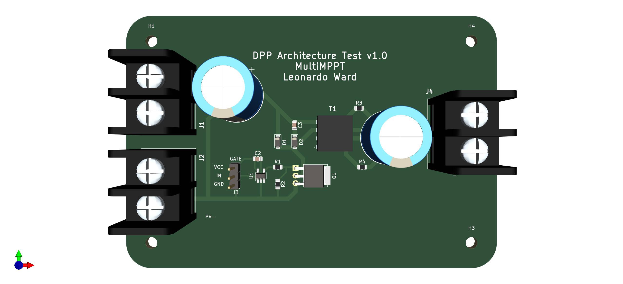
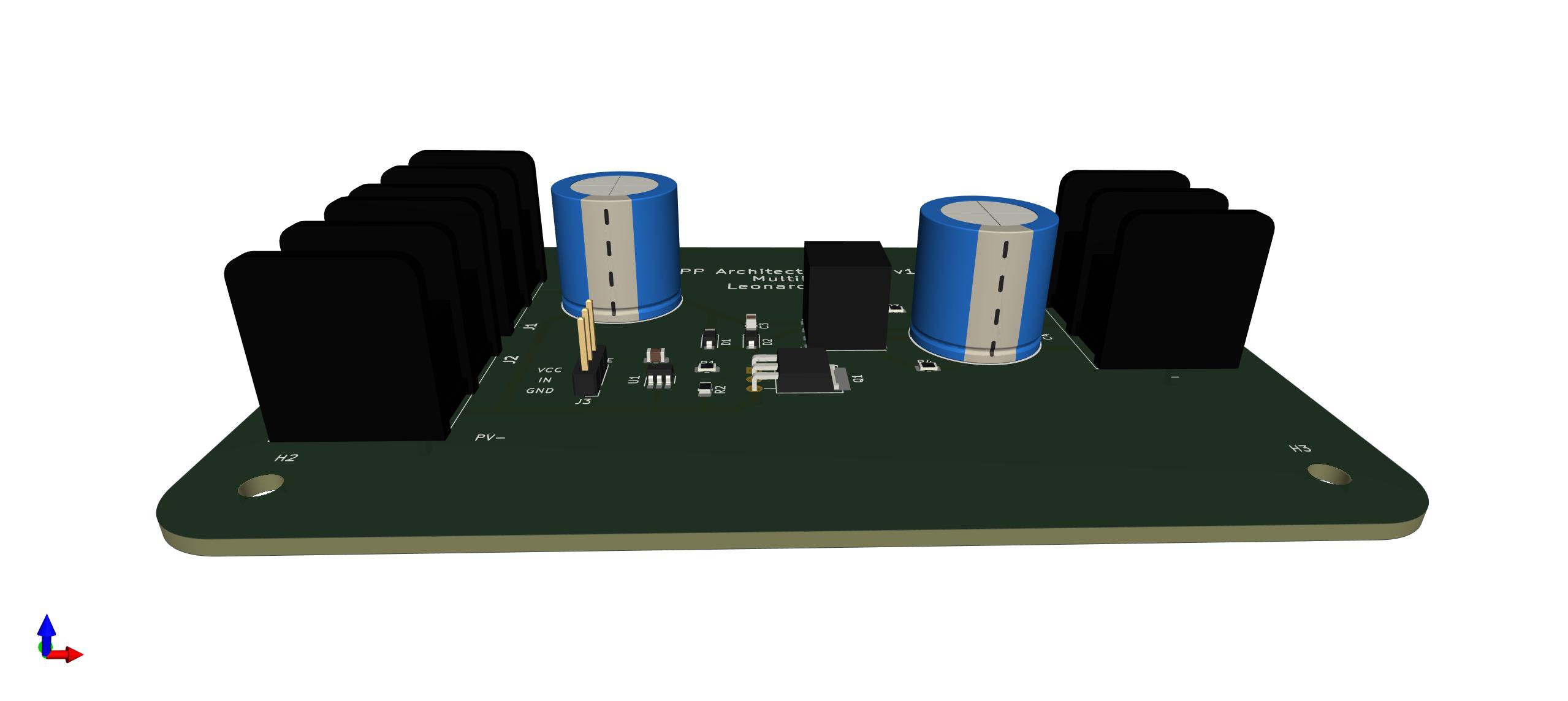
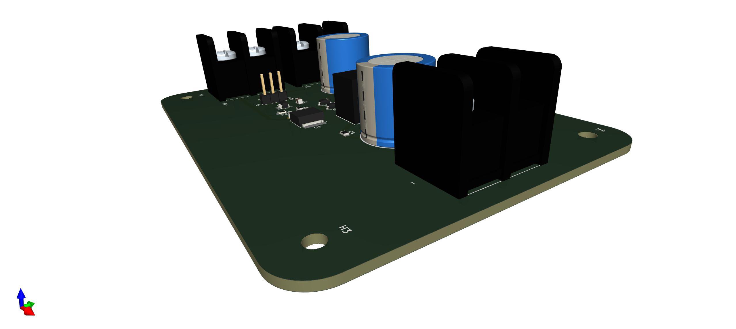
PCB
Bill Of Materials
The overall price is $15.08 (USD), without taking into account shipping costs. This designed could be a cheaper, some components have higher specifications than those that are needed (e.g. power dissipation and current).
Keep in mind that the DPP architecture is not the complete MPPT, but is the most important element in the design (in my opinion) because it allows me to test the efficiency of the system under different conditions, and the use of multiple inputs.
Discussions
Become a Hackaday.io Member
Create an account to leave a comment. Already have an account? Log In.