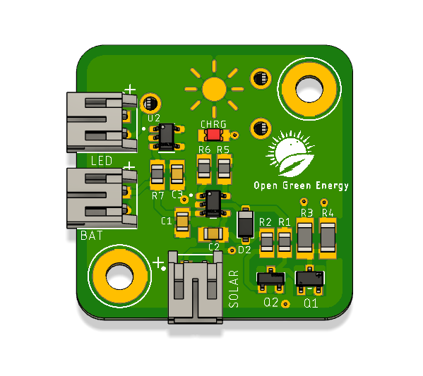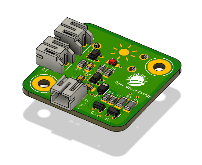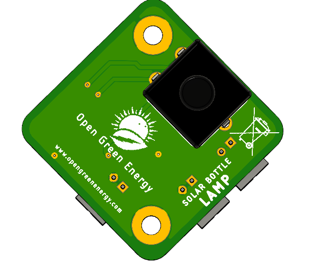


I have drawn the schematic by using Fusion 360 Electronics Design after that switched to PCB layout. I have placed all the SMD parts on the top side of the PCB and the button on the bottom side of the PCB. The main reason for placing the button switch on the bottom side is that it will be easier to access from outside of the enclosure. It also reduces the PCB board size.
I have ordered my PCB from PCBWay and received it within 7 days.
Download the Gerber files from PCBWay
 Open Green Energy
Discussions
Become a Hackaday.io Member
Create an account to leave a comment. Already have an account? Log In.