 John Opsahl
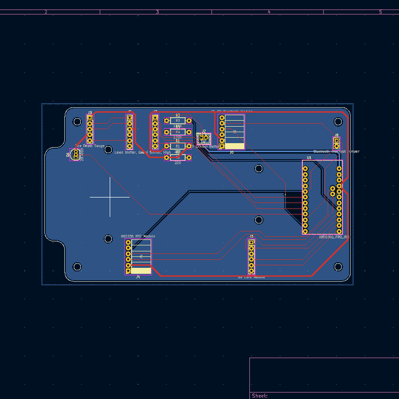
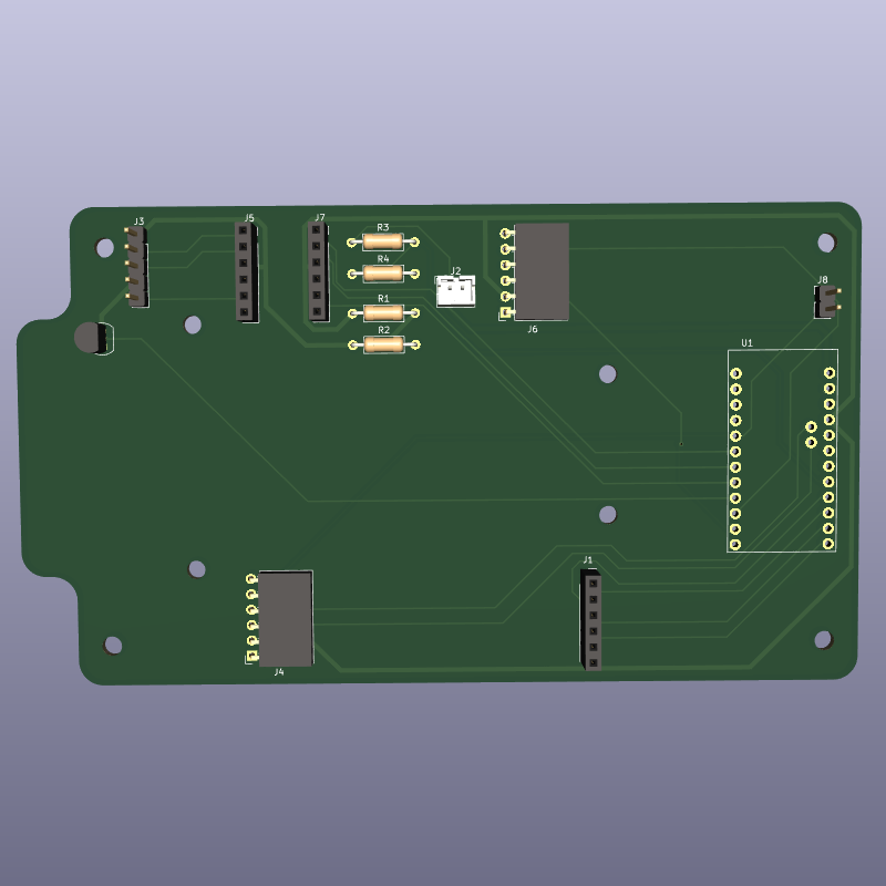
First pass of trace routing for the OpenDendrometer custom PCB is complete. Not a lot of room in the schedule for rework so it is important that this design be near perfect. Fortunately, I am working with low frequency circuits on this PCB design so "near perfect" is more an exercise of "connect the dots" than partitioning component types, establishing keep out zones, and managing return paths. Since component placement on this board is highly dependent on mechanical design there is not much opportunity these strategies anyways.
I often notice that some are scared away from hobby level PCB design because of the perceived complexity of component placement and trace routing. Maybe it is a combination of luck and using prefabbed hobby electronic modules, but I have fat fingered all my hobby PCB designs without issue. Just connect the correct dots, do not overlap traces, and ensure return paths on the ground plane exist. Crossing my fingers that my luck doesn't run out with this scrappy, hacked-together approach on this PCB design.
Discussions
Become a Hackaday.io Member
Create an account to leave a comment. Already have an account? Log In.