iCEBlaster
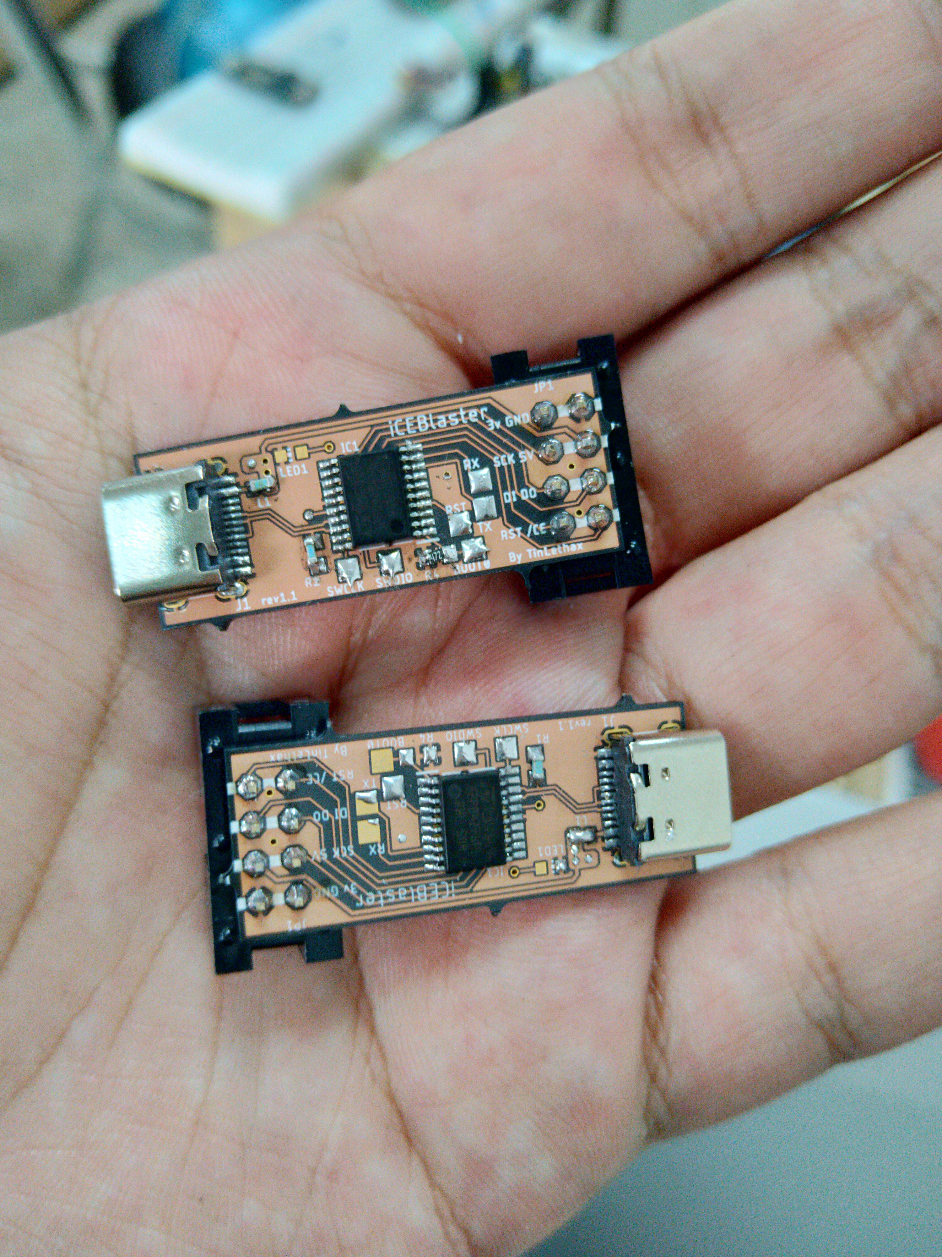
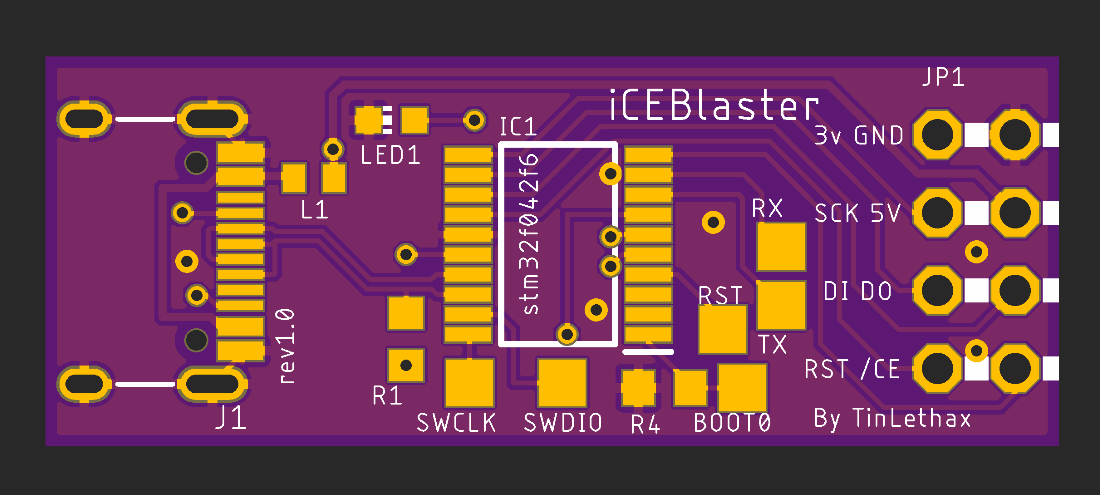
iCEBlaster is a Drag and Drop firmware loader via SPI for iCE40 FPGA. The brain of this project is based on STM32 Arm Cortex microcontroller.
How it works?
Original iCEBlaster (v1) version :
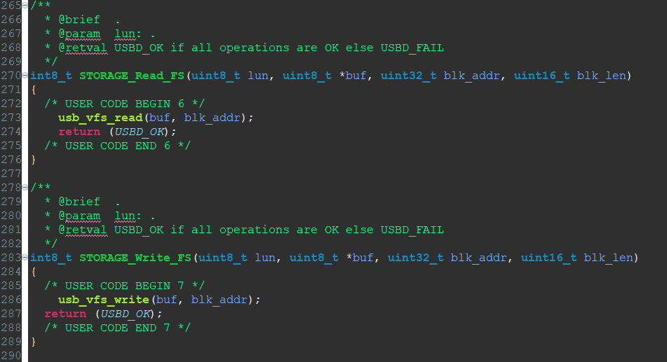
By using USB-FS library working as USB Mass storage device class (USB MSC) and with interface I/O code with internal Flash. Working together as USB Disk pre formatted with FAT12 file system with 1024 Bytes per sector, 64total sectors, 3 sectors reserved for master boot record (sector 0) and File allocation tables(sector 1-2). And using total of 64 internal Flash pages (1Kbytes per page, page 64 to 127, total of 64KBytes). This version of iCEBlaster only support iCE40 with 1K LUTs
By copying the iCE40 FPGA Bitstream to the disk, 2 while loops help to locate the physical address of Bitstream on the internal Flash (for spi tx pointer) and to figure out the Bitstream size (for spi tx size). After that the Bitstream loading sequence begin.
When done, The MCU release CRESET to let FPGA run the firmware that we just flash. Then perform the internal flash reformat to have a new and ready to Drag and Drop USB Disk.
VFS Version :
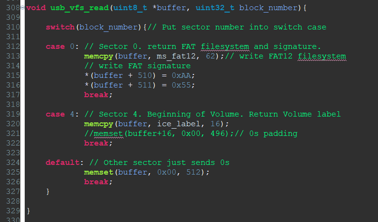
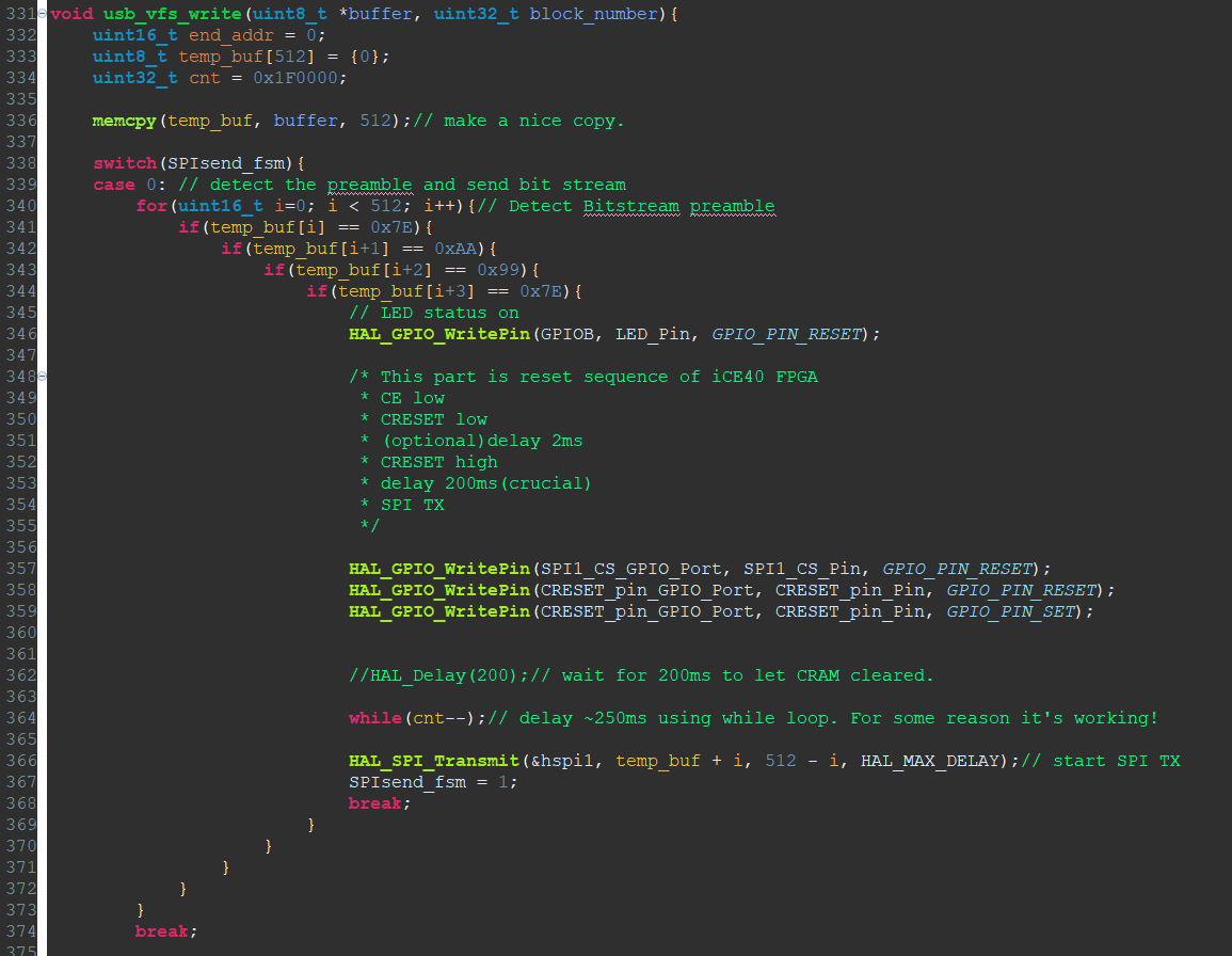
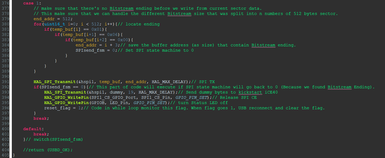
In the VFS version of iCEBlaster. Virtual file system is based on FAT12 and no internal flash was used. The switch case is used to handle all possible sector number to return the correct data (e.g. FAT file system and FAT signature in boot sector, Volume label). And state machine is used for match-detecting the Bitstream from data packet sent from USB Host. And immediately send the Bitstream over SPI in the chunk of 512 Bytes. VFS FAT12 has 512 Bytes sector, Total of 512 sectors, 3 sectors (0-2) reserved for FAT file system and FAT table. Volume label start at the beginning of sector 3. Total of roughly 160Kbytes virtual disk space.
The Bitstream transfer happen after STM32 receive data from USB Host.
The benefit of using VFS is that you can send virtually any Bitstream size. This allow iCEBlaster to not only support just iCE40LP1K and UL1K. But other higher density iCE40 can now be used with iCEBlaster. Plus, when not rely on Internal flash. This doesn't wear out the flash and kills the STM32 fast.
Bitstream locator (iCEBlaster v1)
with while loop and nested if-statement to check for magic word (or preamble) 0x7EAA997E. This is the beginning of the Bitstream. Another while loop check for 0x010600 which indicates the end of Bitstream (and It's actually a wake up command to wake the iCE40 up).
iCE40 Bitstream Loading sequence.
// Enter Slave SPI mode.
1. Set SPI CE pin to LOW.
2. Set CRESET pin to LOW.
3. Wait for 2ms.
4. Set CRESET pin to HIGH.
5. wait for 200ms to let CRAM clear itself.
// Send Bitstream
6. Send Bitstream Via SPI, 8 bit and MSB first.
7. Send additional 12 dummy bytes (96 clock cycles).
8. (optional) send additional 7 dummy (56 clock cycles), this will allow configuration SPI pins to reuse as user PIO.
// End of Bitstream loading.
9. Set SPI CE pin to HIGH.
 TinLethax

 Jesse
Jesse
 sphaleron
 Stephen Holdaway
 Necromant
Can the ICEBlaster be switched back and forth from being a VFS FPGA Drag and Drop firmware loader to just a STM32 uC / USB-C dev board?