 deʃhipu
Today I couldn't sleep, so I did what I do when I can't sleep: designed a PCB. As I previously mentioned, version 2.0 is very close to what I want, but there were some small details I wanted corrected. Those changes are not really enough to warrant a whole new version, and I'm not going to do a new certification for it.
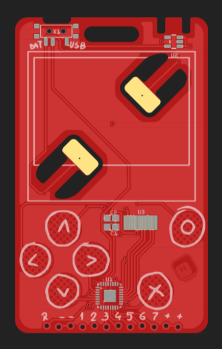
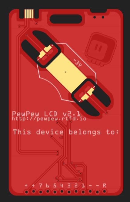
I removed the unused resistor footprint, and moved the capacitors away from pads, so that they don't get in the way. I centered the display, so it will now fit the outline properly. I moved around the traces for the touch pads, so that you are less likely to touch a trace and activate a touchpad when you didn't mean to. I removed the doodles to make it look a bit cleaner, and on the back I added a place to sign the device, to make it more personalized. I also covered the expansion connector pads with soldermask, so you are less likely to touch exposed solder with your fingers.
I will order the PCBs from @Elecrow once again, and I will publish the design files once I have tested and verified that they work.
Discussions
Become a Hackaday.io Member
Create an account to leave a comment. Already have an account? Log In.