 zpekic
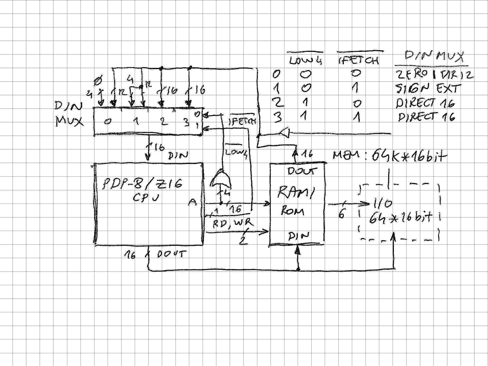
The picture illustrates a simple way to force a PDP-8/Z16 system into "compatible" mode. As this is a theoretical/or maybe FPGA implementation, system bus can be designed in non-multiplexed way, with DIN (data in) and DOUT (data out) buses separated.
Some notes about the schematic below:
- DIN mux is supposed to feed instructions and data into CPU seamlessly if accessing "extended flat memory" (above 4k word), and if accessing PDP-8 basic 4k words, differentiate between instructions (force upper 4 bits to 0000 for "compatibility") and data (assume 2's complement so extent bit 11 to 12..15)
- DOUT goes directly as 16 bit to I/O and memory
- I/O can - based on actual device - be hooked up to any part of the 16-bit data bus, for example 8-bit devices could work on D7:0 or D15:8 etc.
Discussions
Become a Hackaday.io Member
Create an account to leave a comment. Already have an account? Log In.