 zpekic
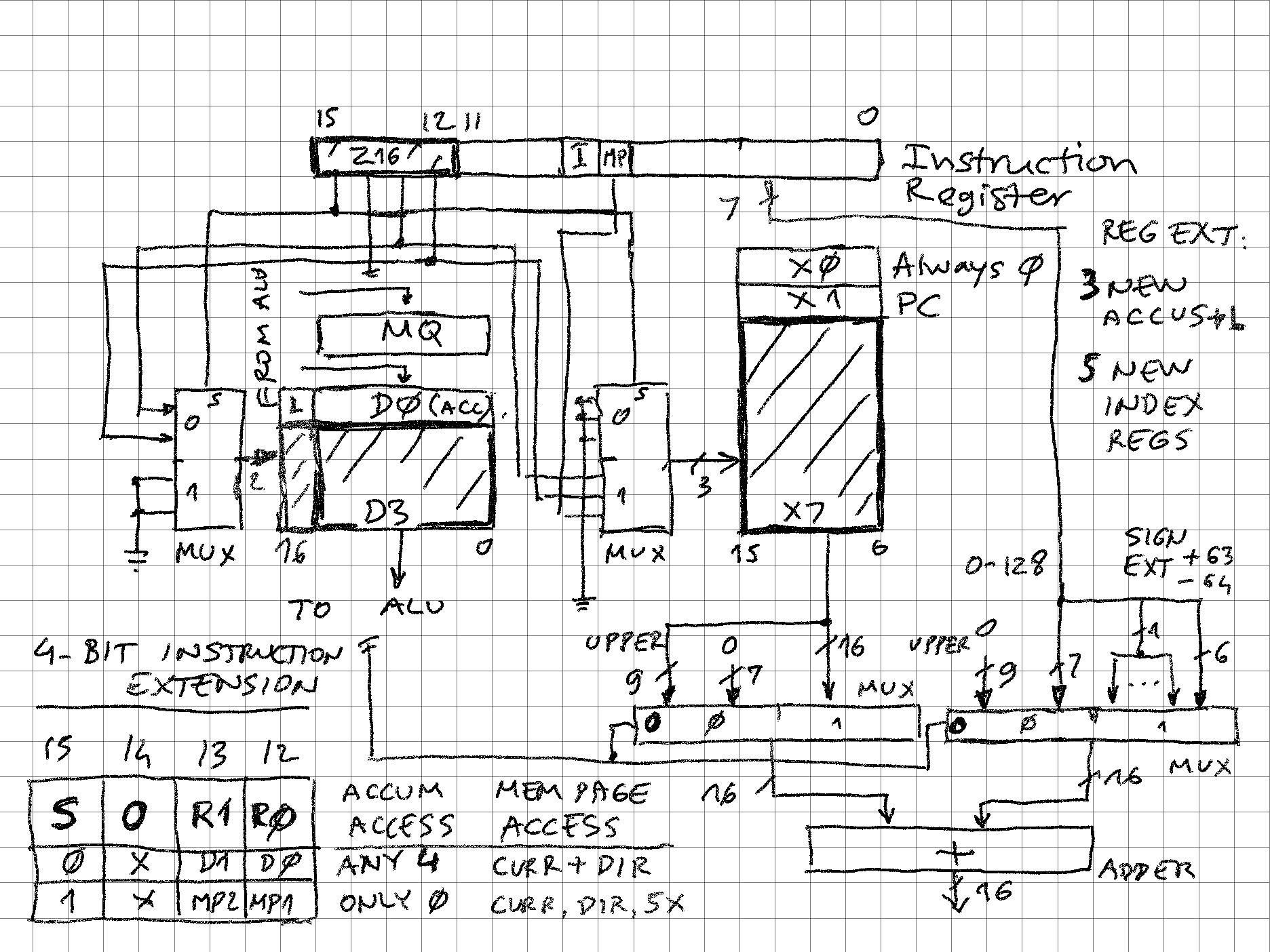
The schema below illustrates the additions to CPU programming model and how they are activated by the upper 4 bits of the instruction register. Some notes:
- Microcode (or state machine) driving the instruction execution has no knowledge of the registers being used - it will use ACC/L or PC, or any X (index register) as the selection happens by pointing to 1 out of 4 or 1 out of 8 purely in hardware
- ACC/L mux - based on IR15 (S), either ACC/L(0) will be selected, or any of 4 given by IR13:12
- Once ACC/L is selected, rest of hardware (mostly ALU) sees 1 ACC/L exactly like in the legacy PDP-8
- X mux - based on IR15 (S), selection is either 0:0:MP or X2:X1:MP - because direct page register is mapped to X0 and PC to X1, changing S bit on the fly from one instruction to another does not disrupt the program flow
- X0 and X1 (zero, PC) are modified directly by microcode, so a bypass / force needs to be implemented on X mux but for simplicity is not shown below
- X0 can be used at T (temporary) register - as long as during memory address calculation for memory reference instructions is set to 0. Typically, a microinstruction step would clear it to 0 before instruction execution phase
- For memory reference instructions, first step is to evaluate the X + offset. IR14 (O) bit allows two ways to evaluate this - either "legacy" page|offset concatenation or real 2's complement addition. 2 muxs handle this - one taking X register value and the other the offset from IR
Discussions
Become a Hackaday.io Member
Create an account to leave a comment. Already have an account? Log In.