Now that my semiconductor forge is (mostly) built, it's time to start actually building some PN junctions!
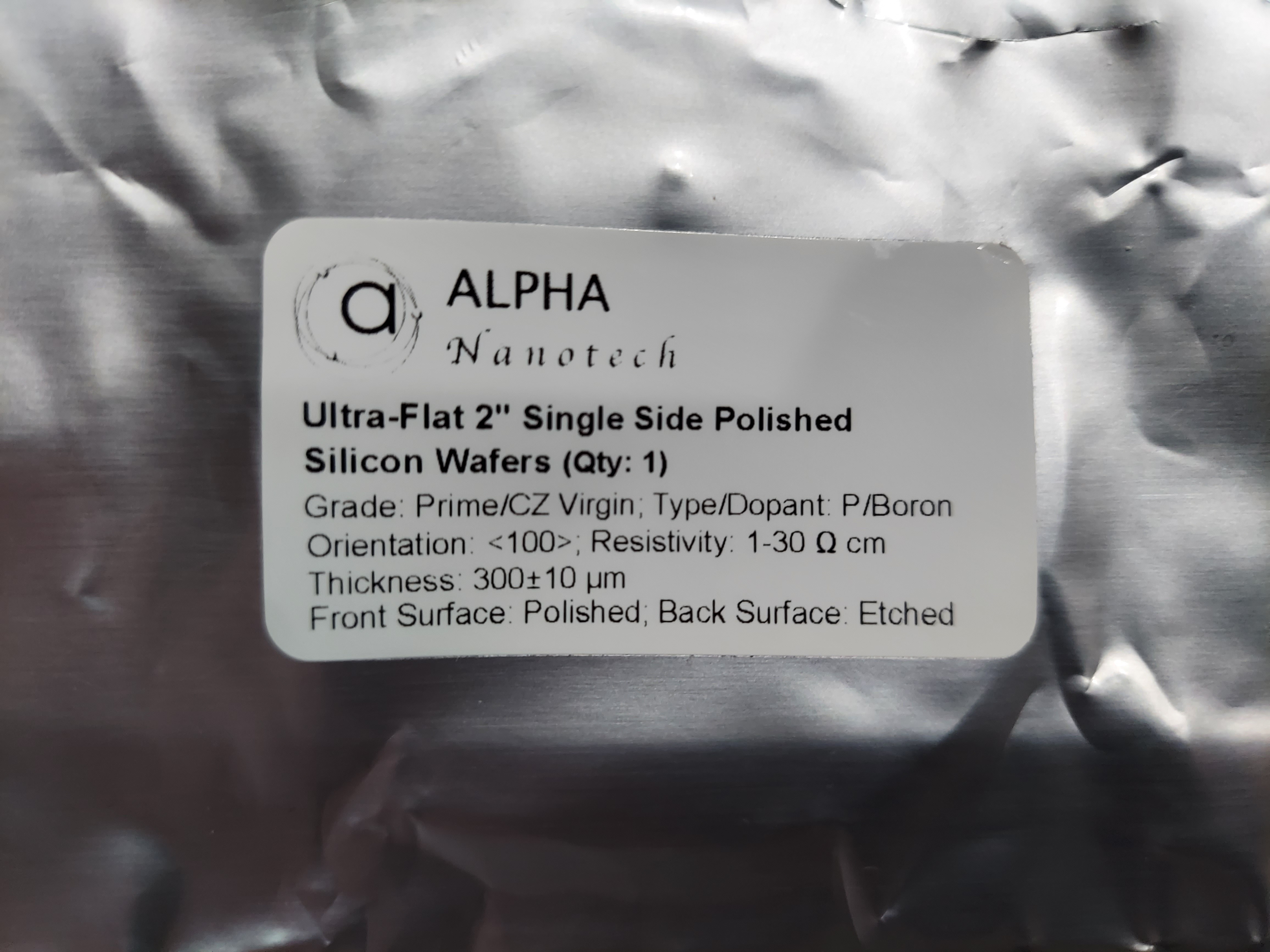
There are several things I'm going to have to do correctly in order to get this right. I've been experimenting with a P-Type wafer for a few days now.
Here's some initial notes:
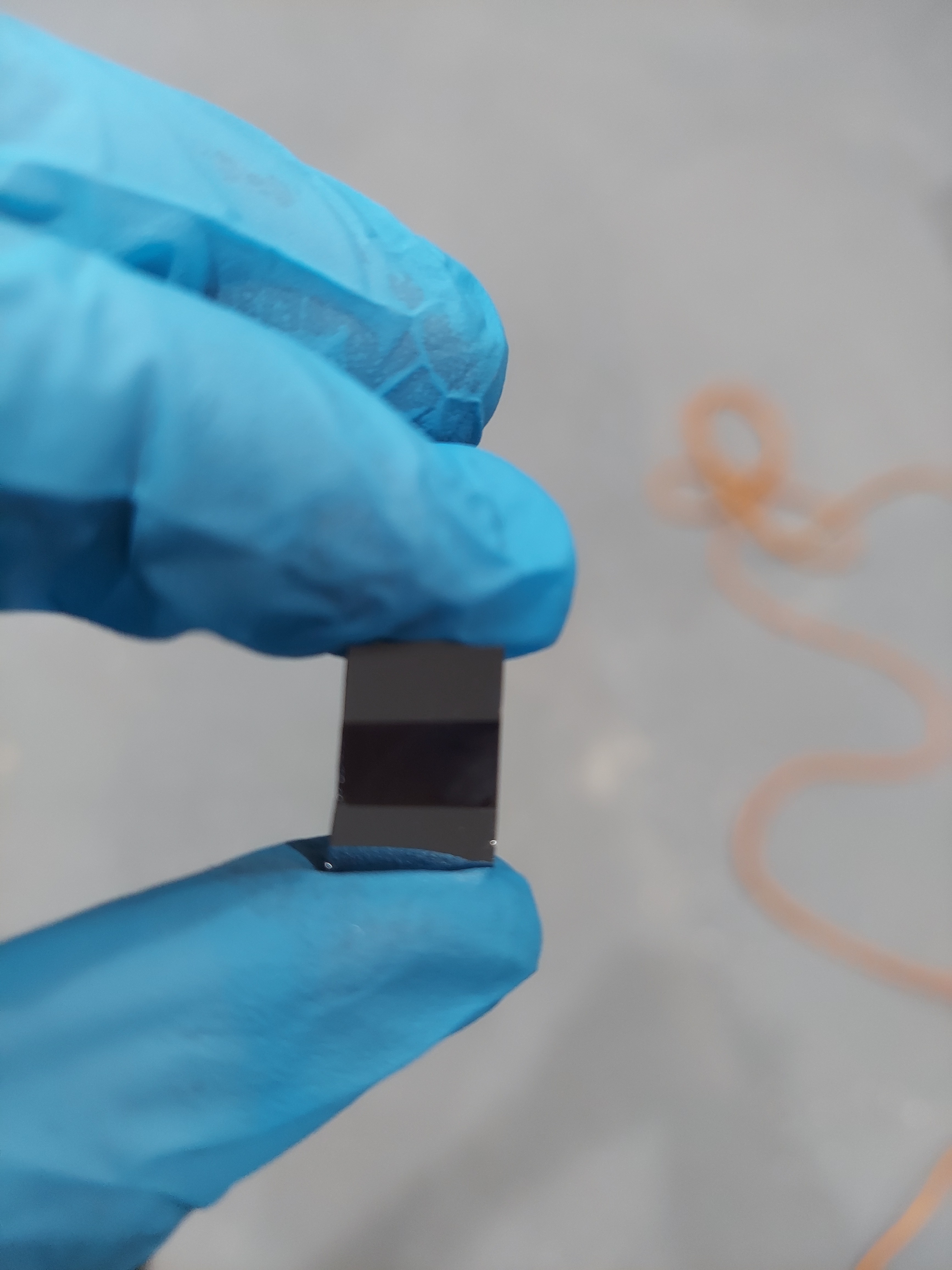
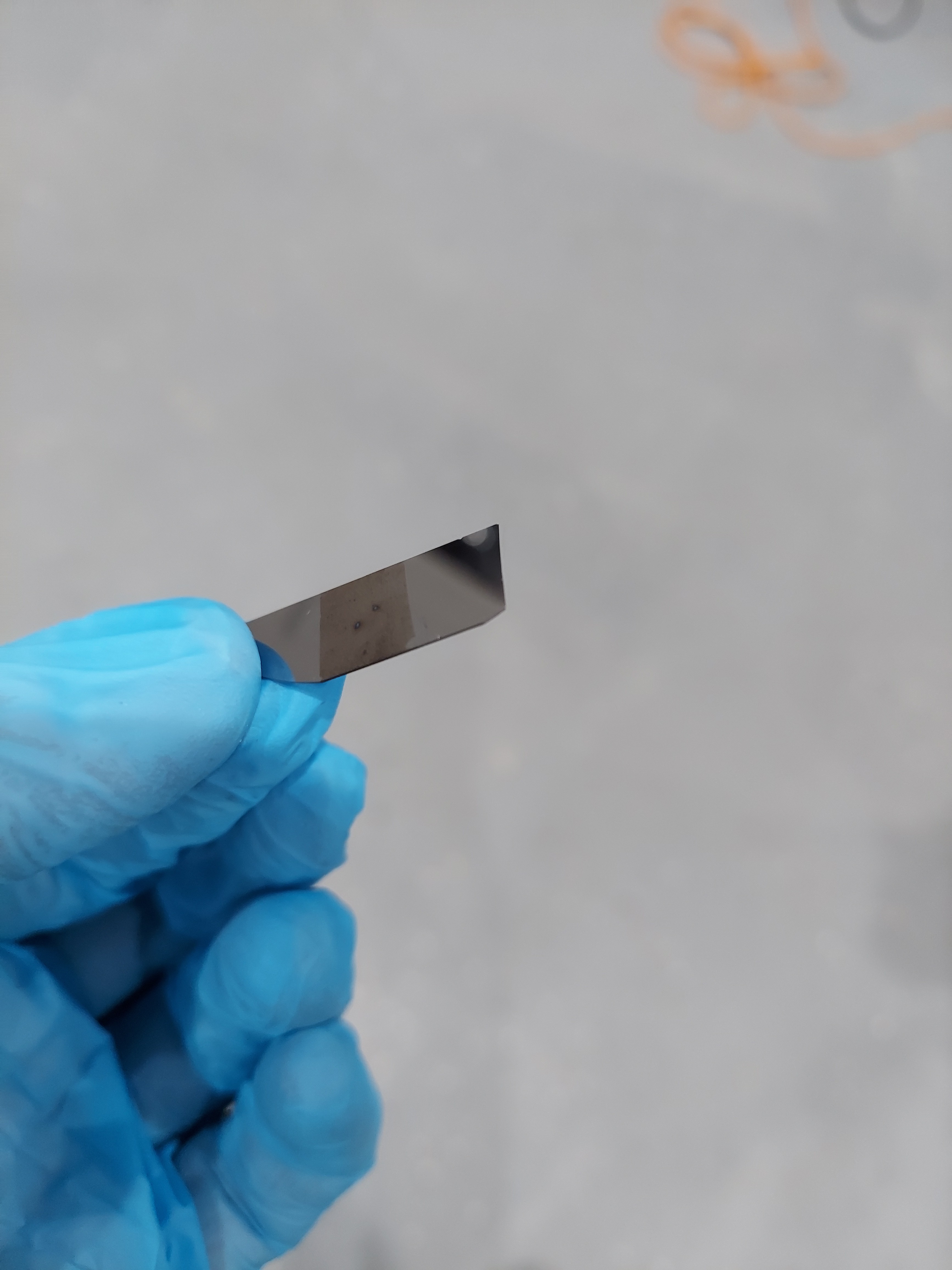
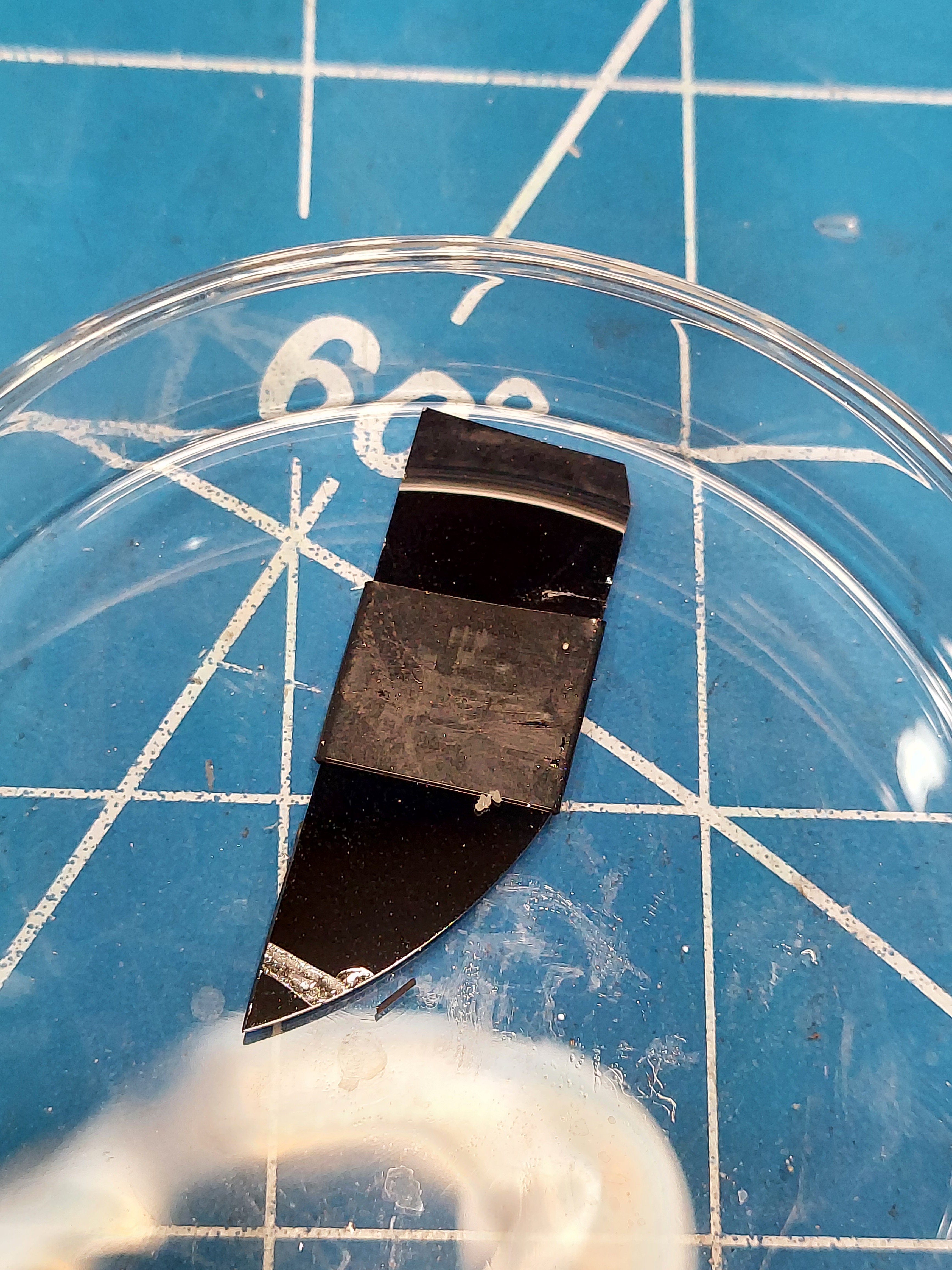
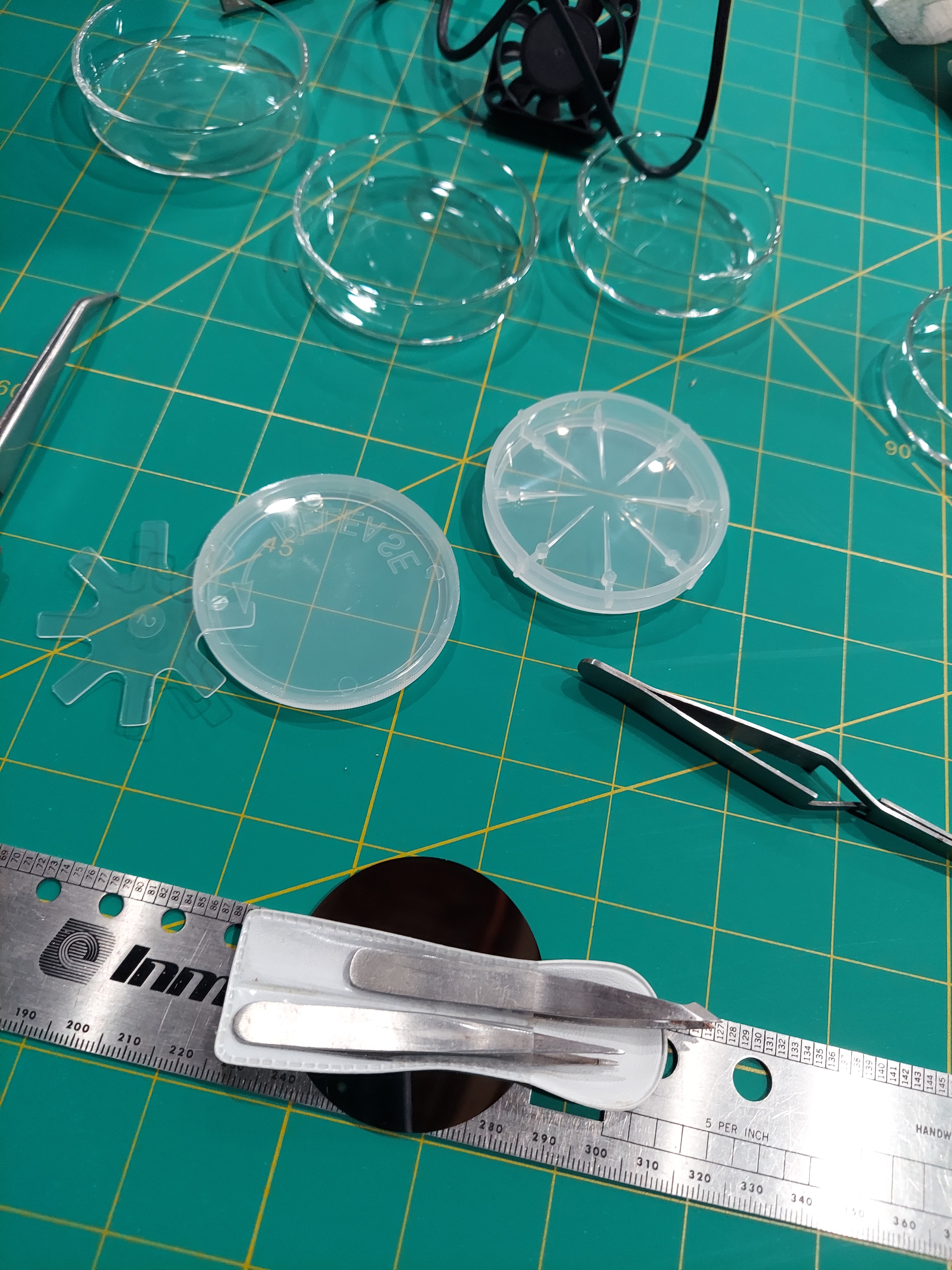
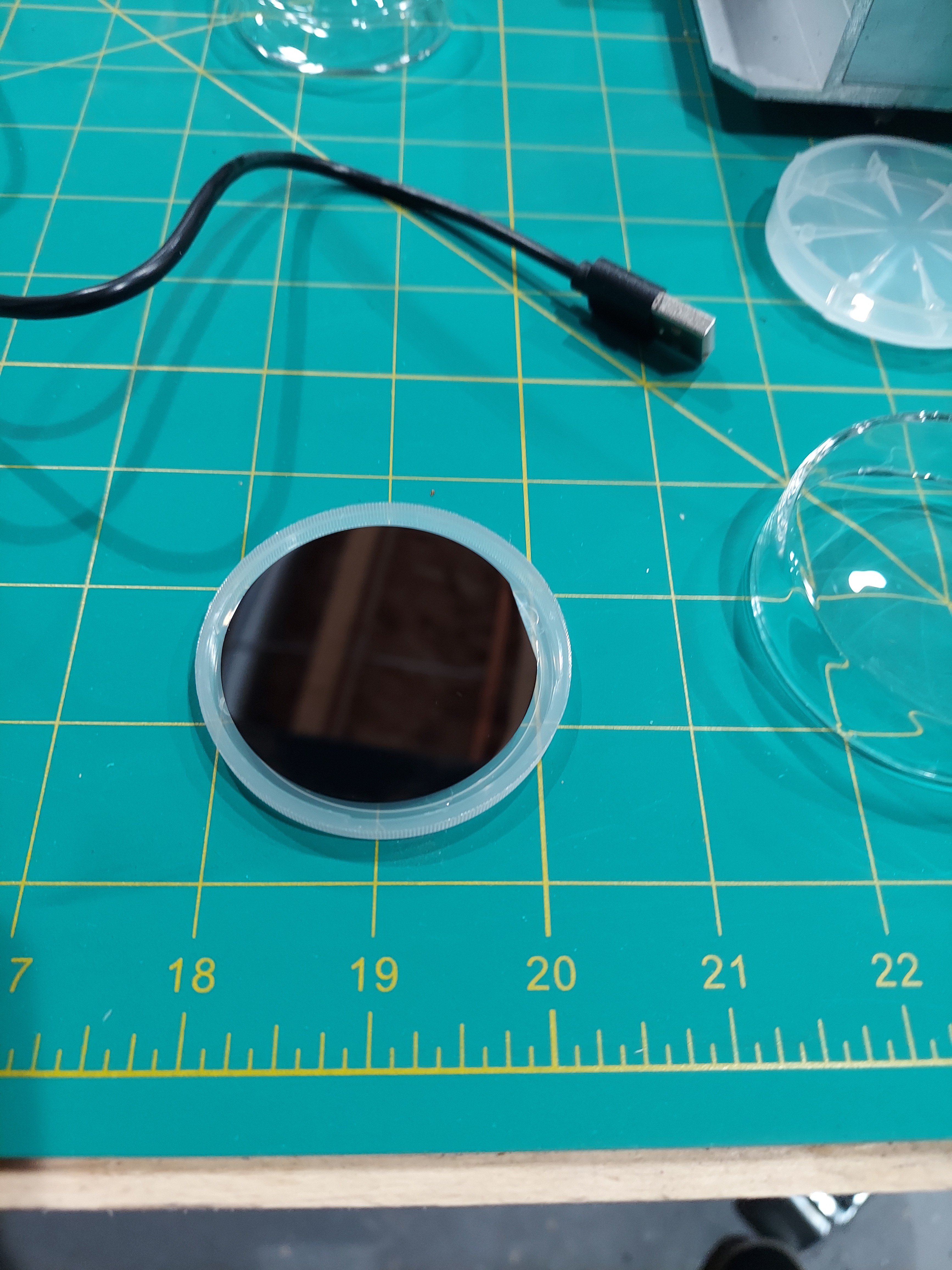
- Breaking the silicon is more tricky than it looks. My first 2" wafer shattered leaving only a few sizeable working pieces.
- Growing oxide layers - I downloaded and printed the silicon dioxide growth rate chart (https://cleanroom.byu.edu/oxidetimecalc) and used the calculator to estimate growing oxide layers of different thicknesses. My furnace can blow water mist over the chips for increased oxide growth.
- Working with Chemicals!
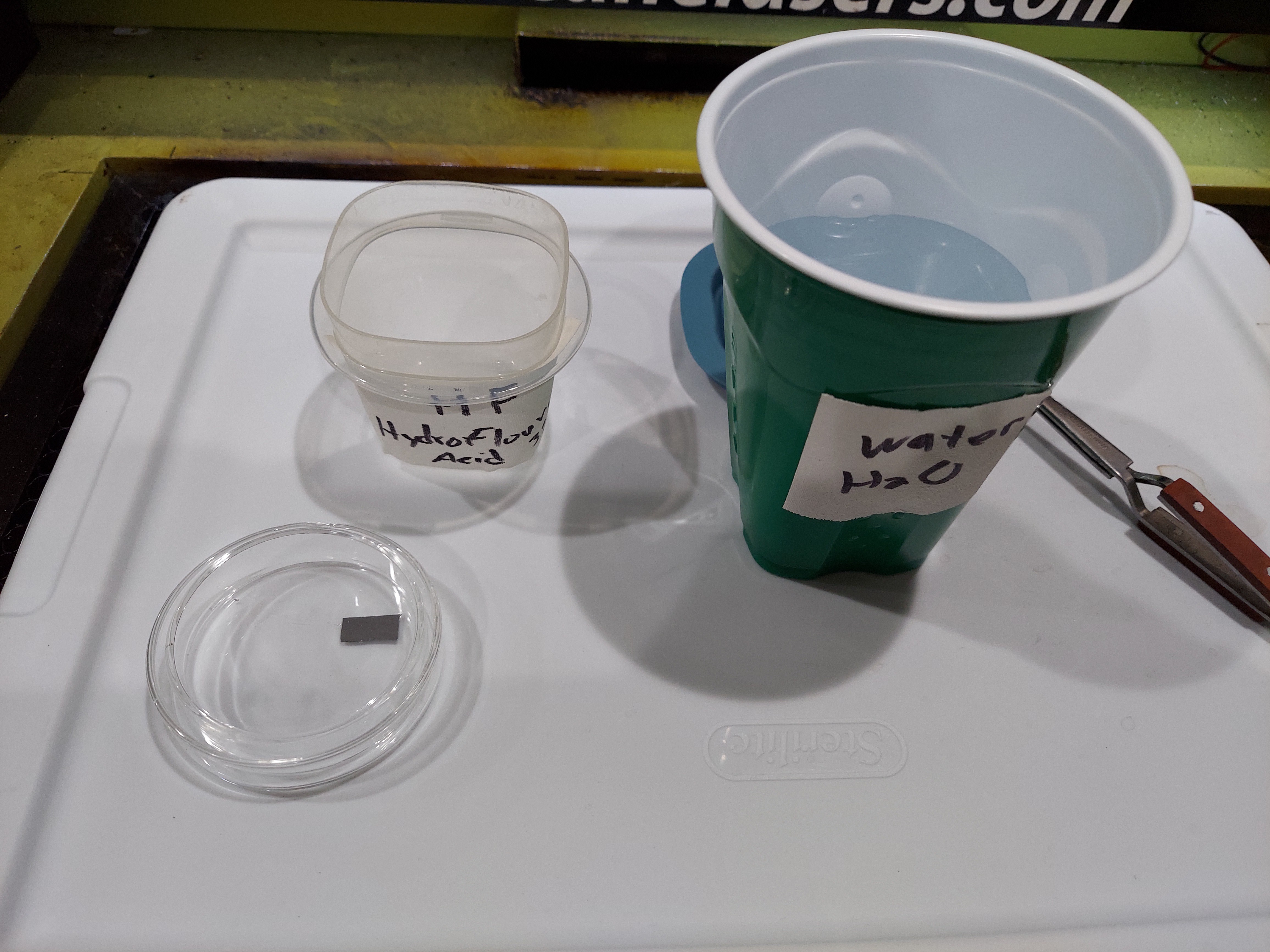
- Hydrofluoric acid is some pretty nasty stuff.
- You need to wear safety gear when using chemicals.
- You need a ventilation system - luckily I thought of that when I built my lab.
- You're going to need to collect few essential chemicals to make this all work
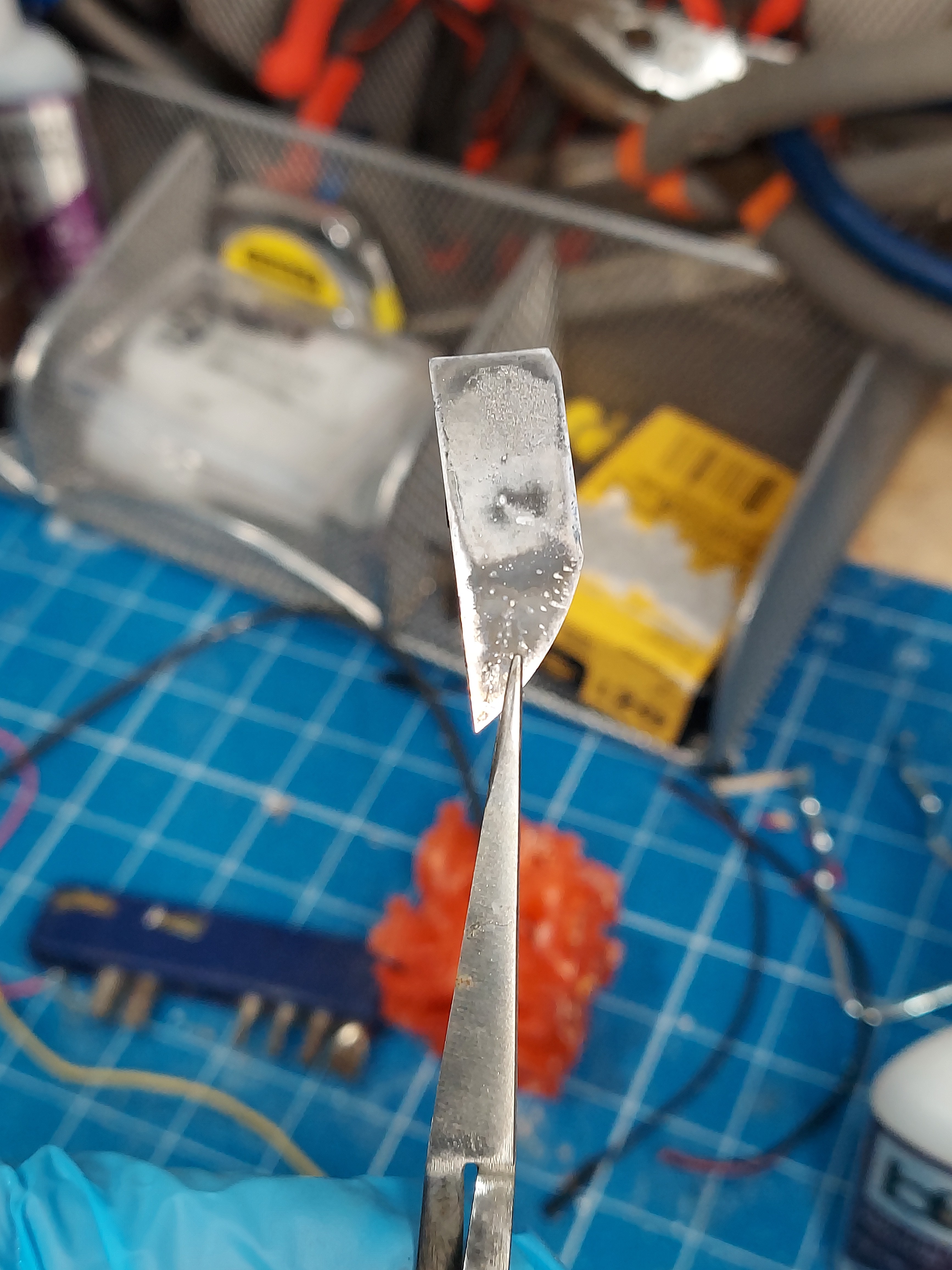
- Etching Silicon dioxide layers!
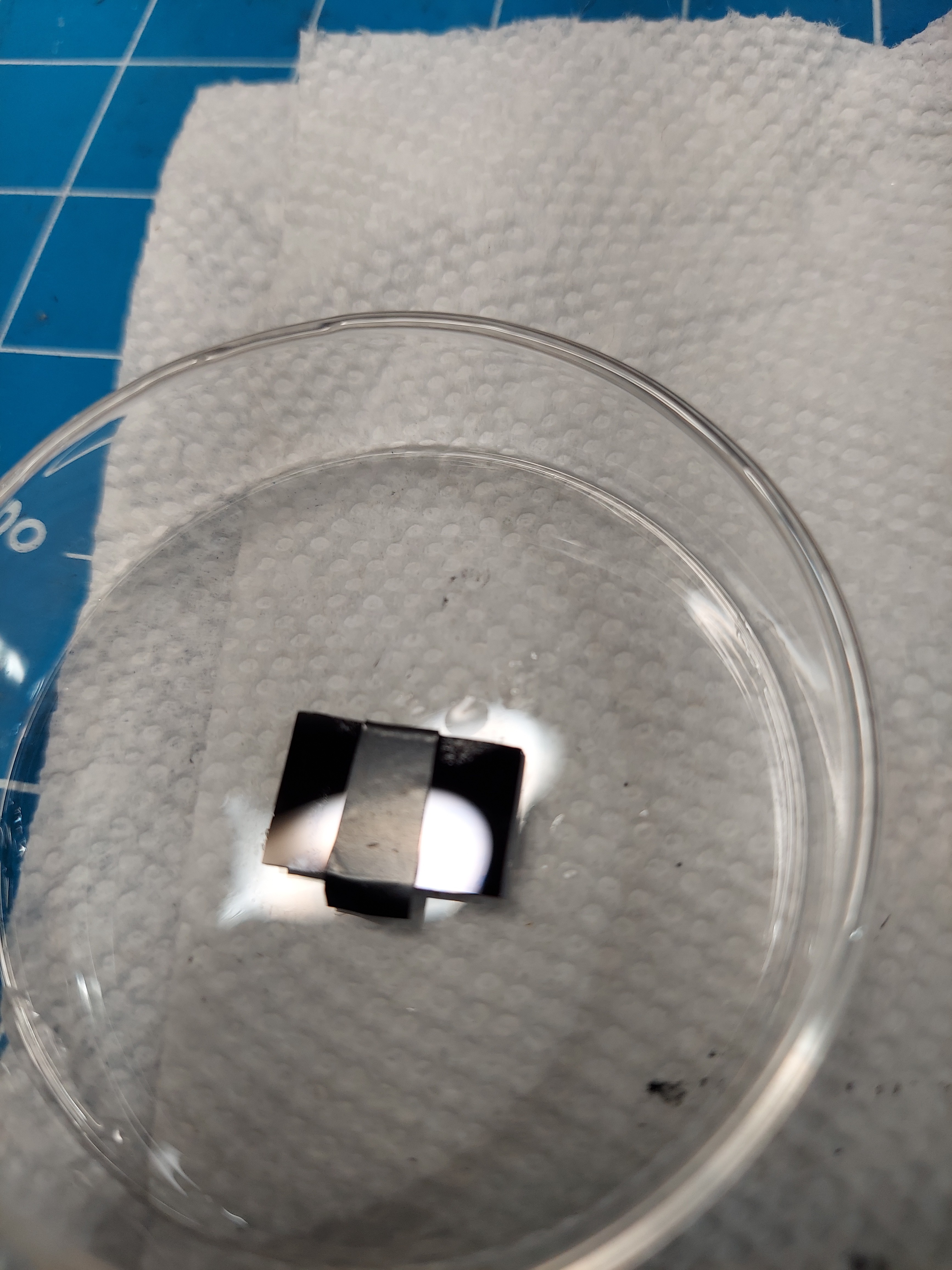
- Masking systems
- Photoresist (positive and negative)
- SLA UV resins can be used along with UV DLP and UV laser systems. I'm starting to experiment with these and getting some positive results.
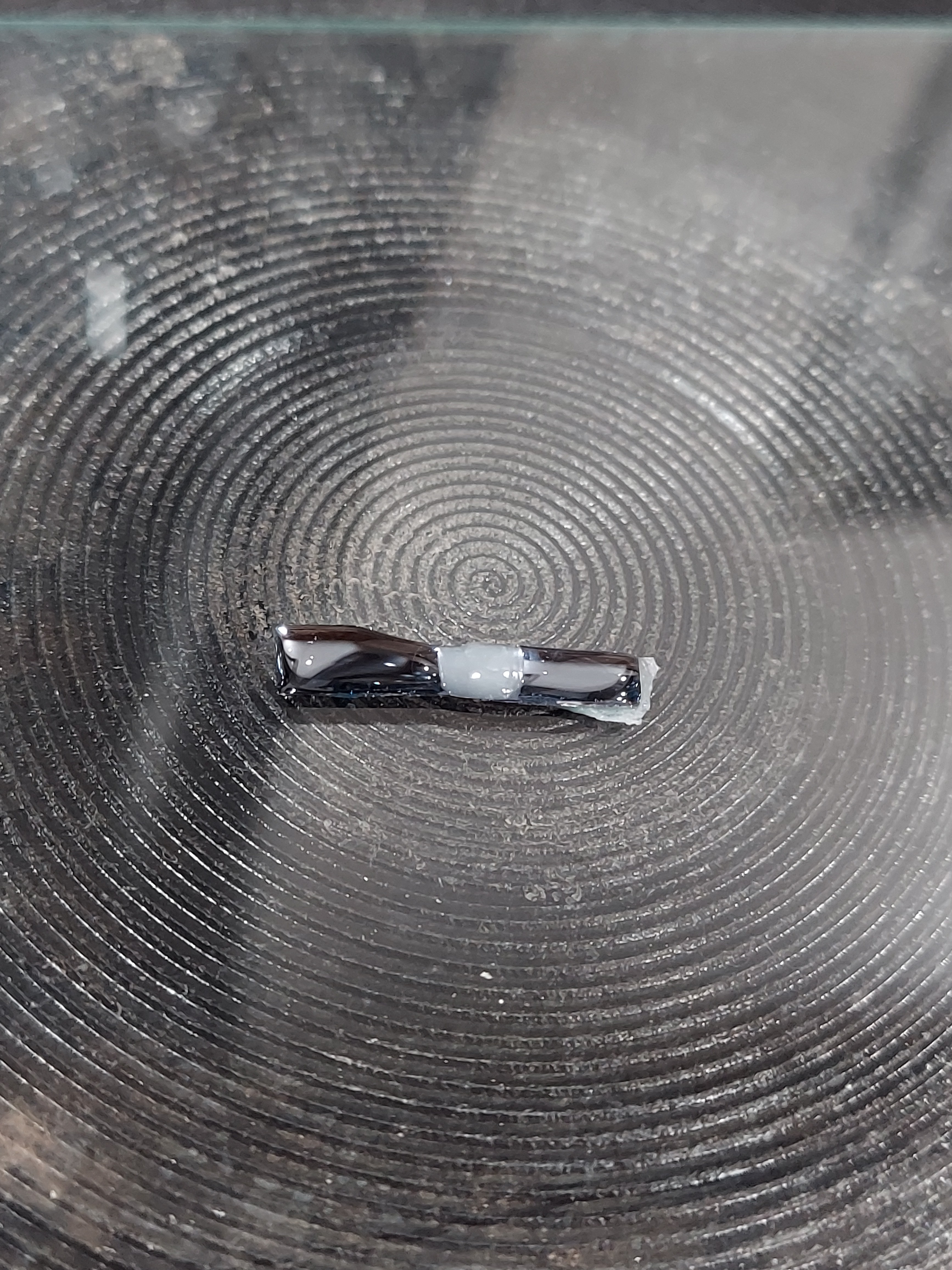
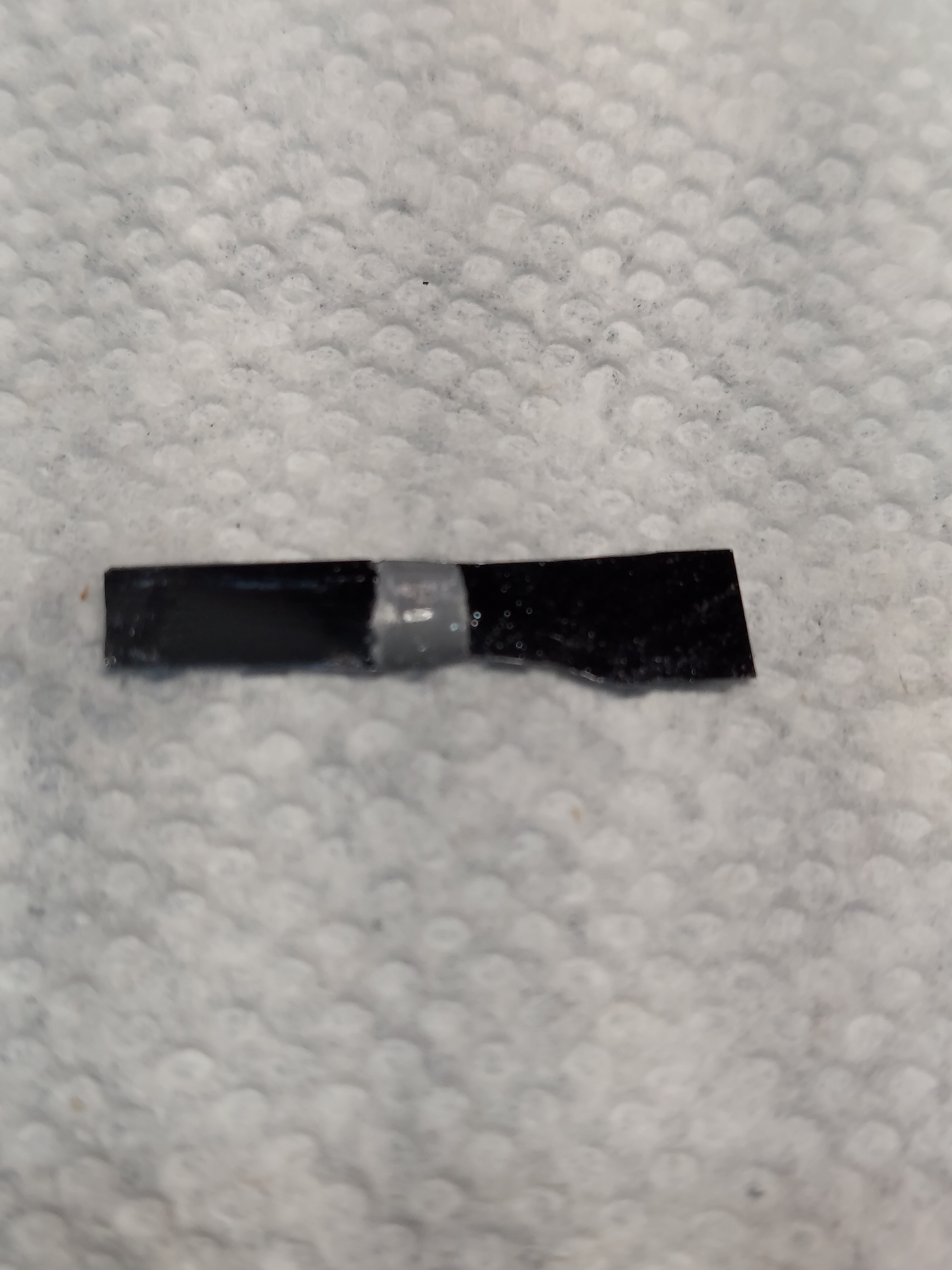
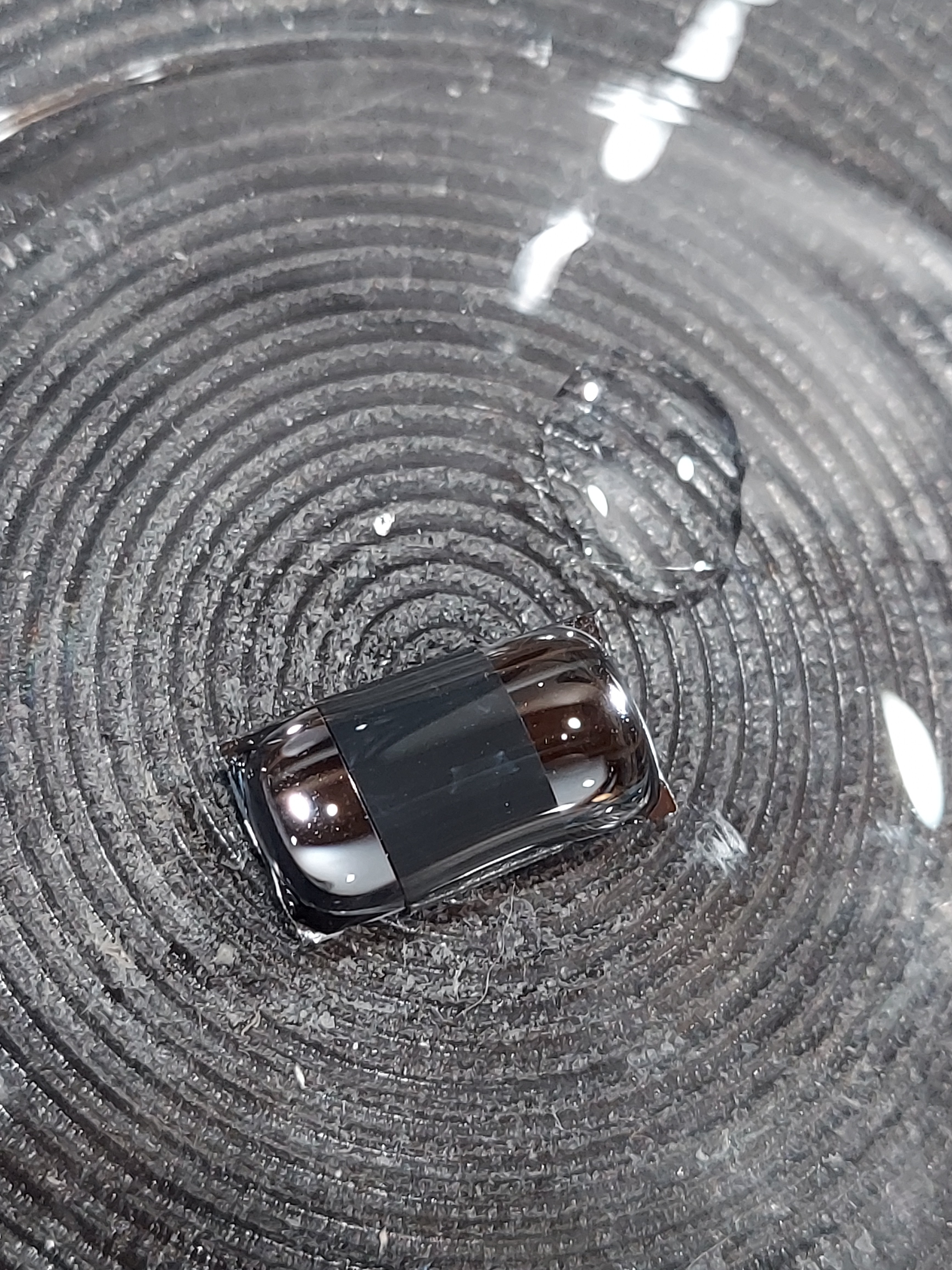
- Black electrical tape cut with a razor (What I'm starting with)
- Masking systems
- HF acid is used to etch the silicon dioxide layers
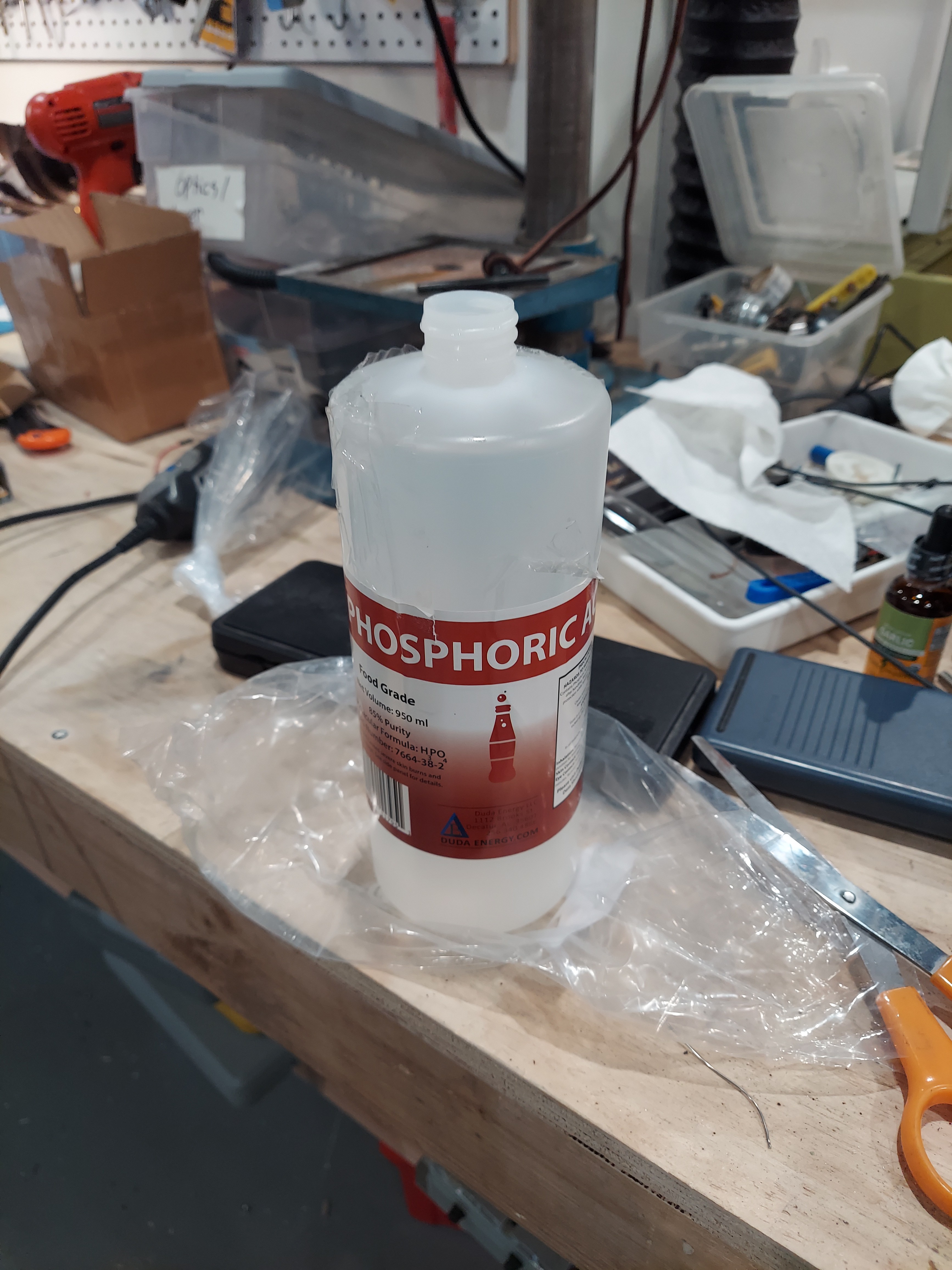
- Using dopants! So - I bought a bottle of 85% Phosphoric acid to use ad an N-Type dopant. I also bought boric acid powder. Neither were hard to find or too expensive.
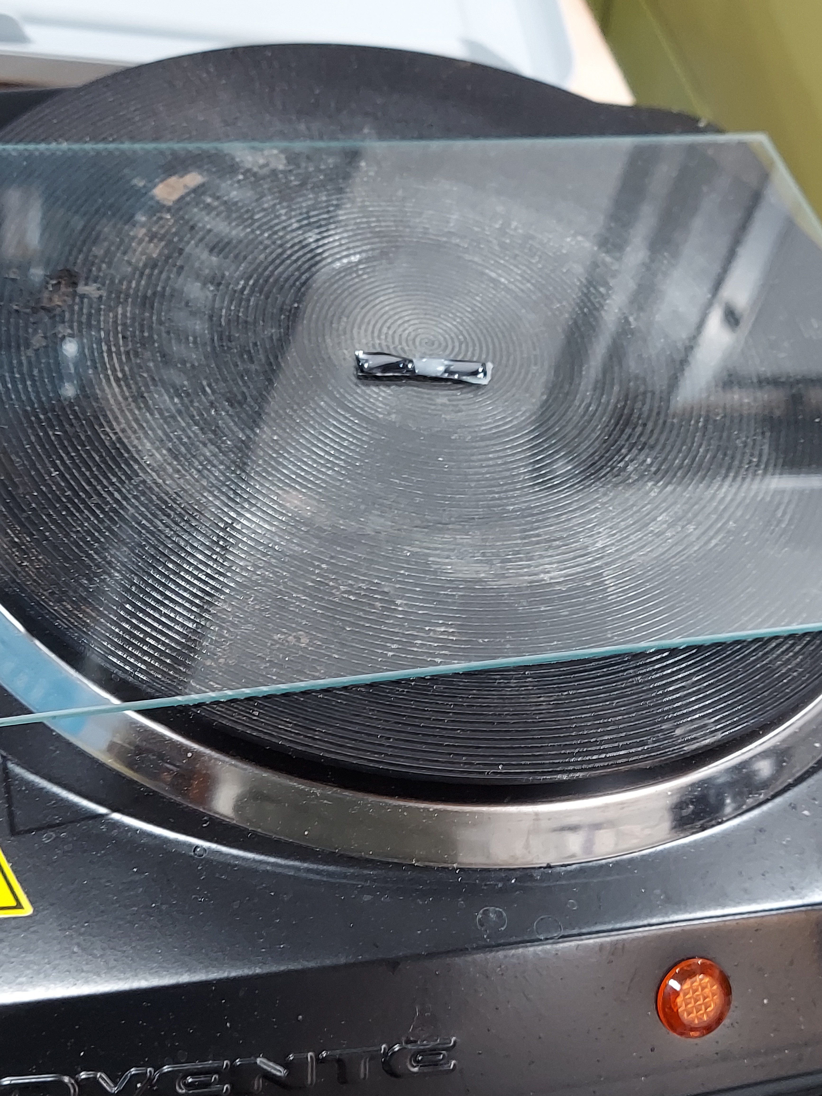
- So far - I have simply put a few drops of phosphoric acid on a pieces of silicon and baked it in for an hour at 1000c. Results have been very promising!
- Measuring and testing
- I'm a big believer in documenting and recording results.
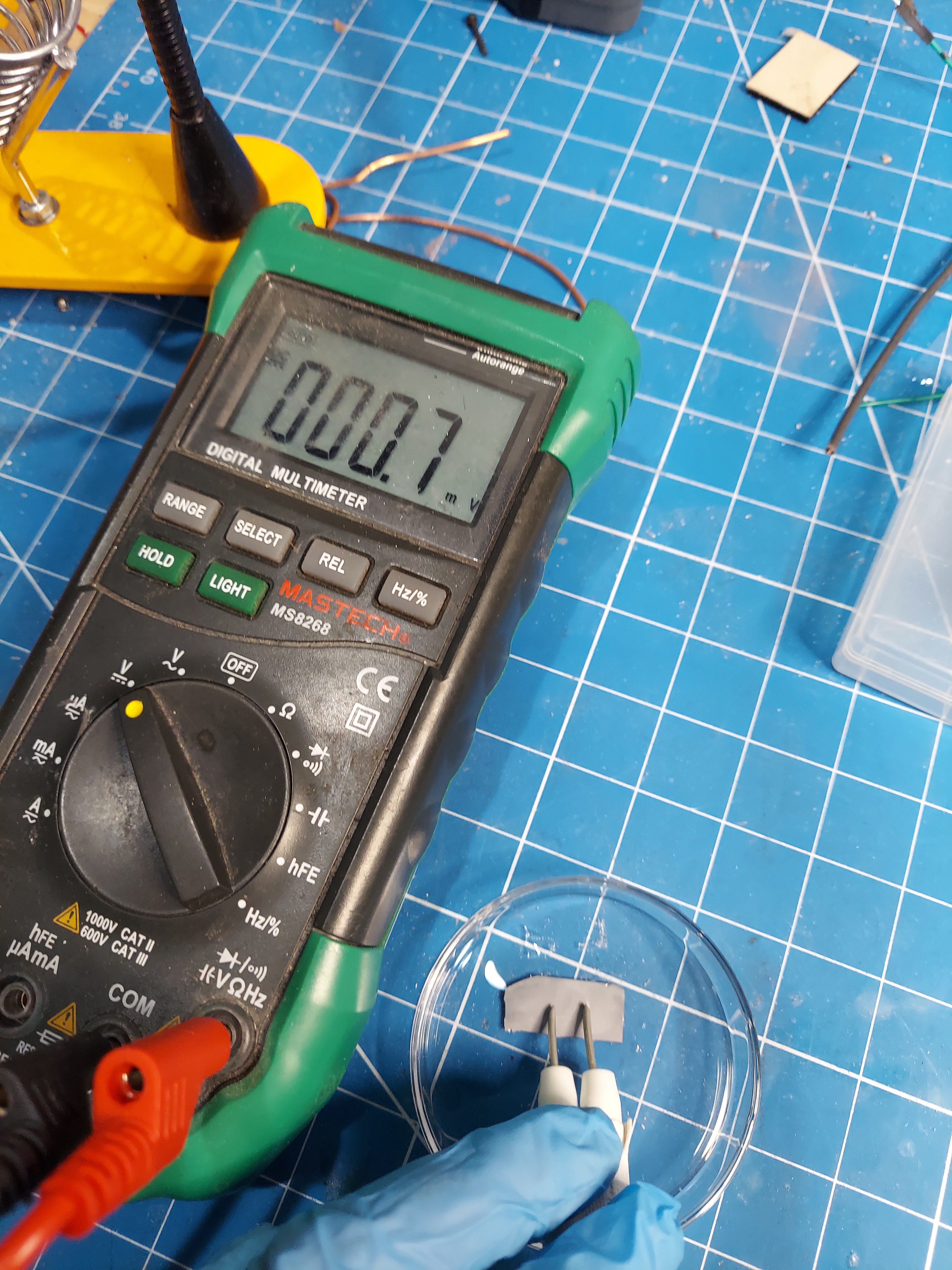
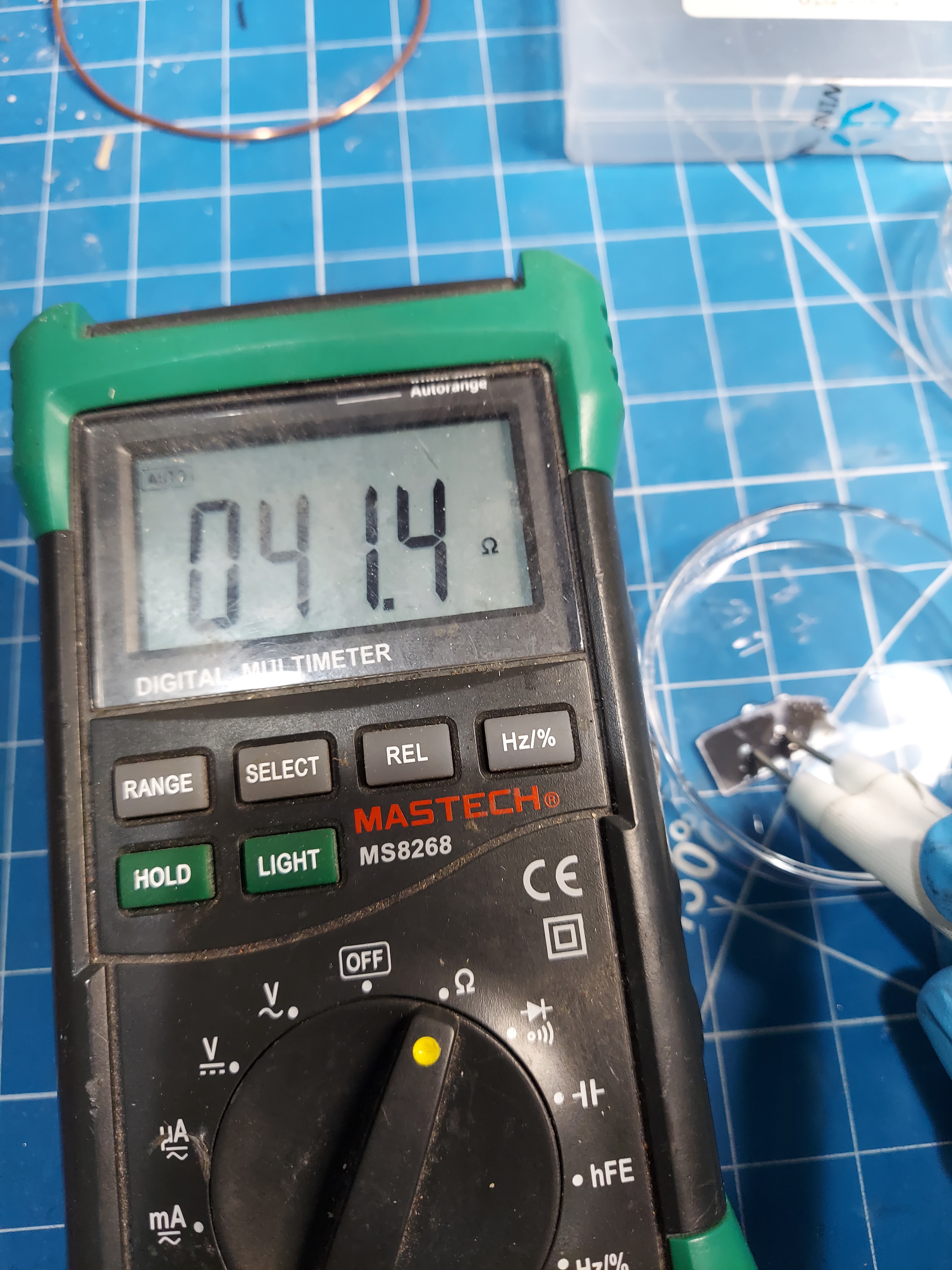
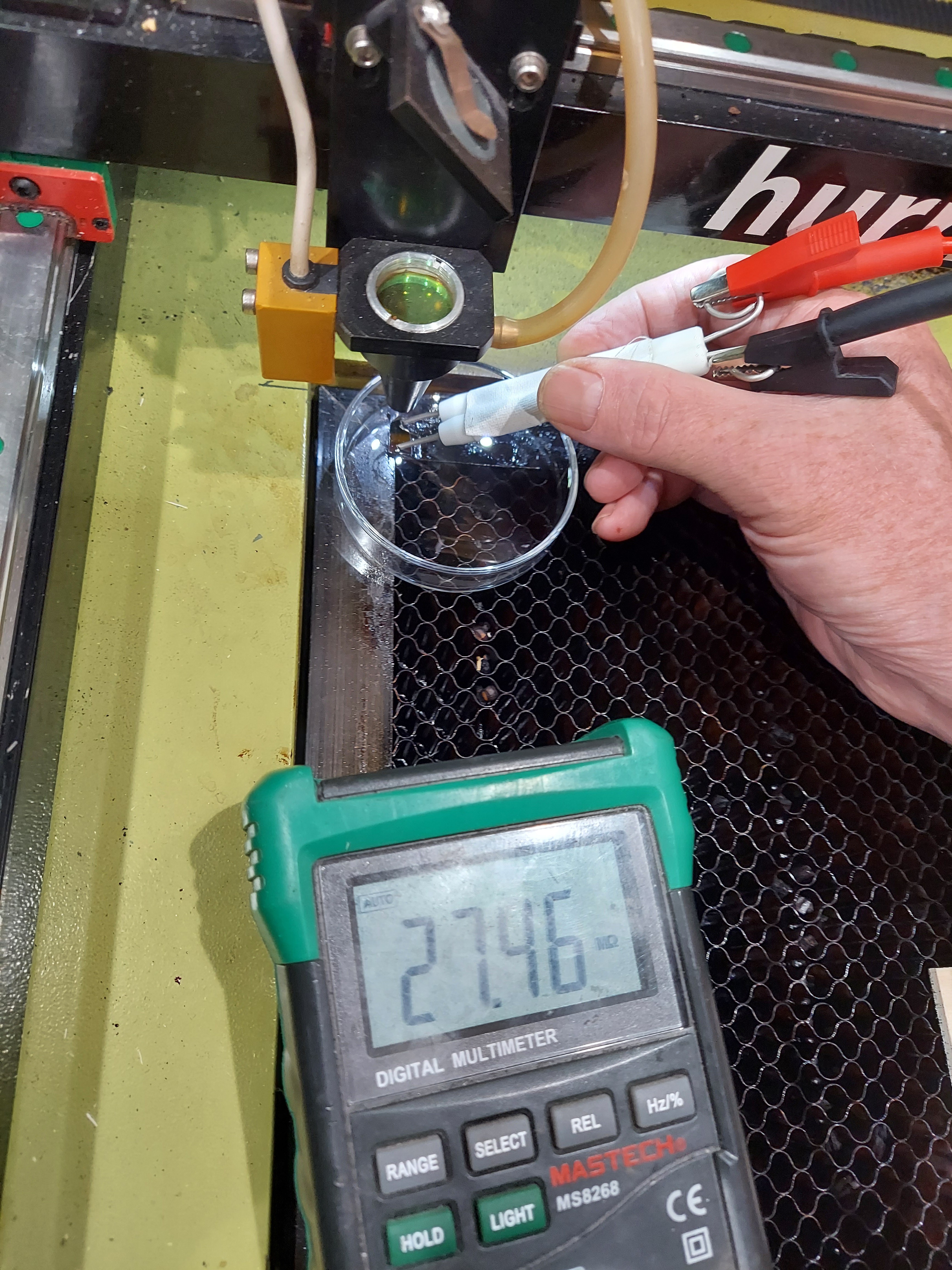
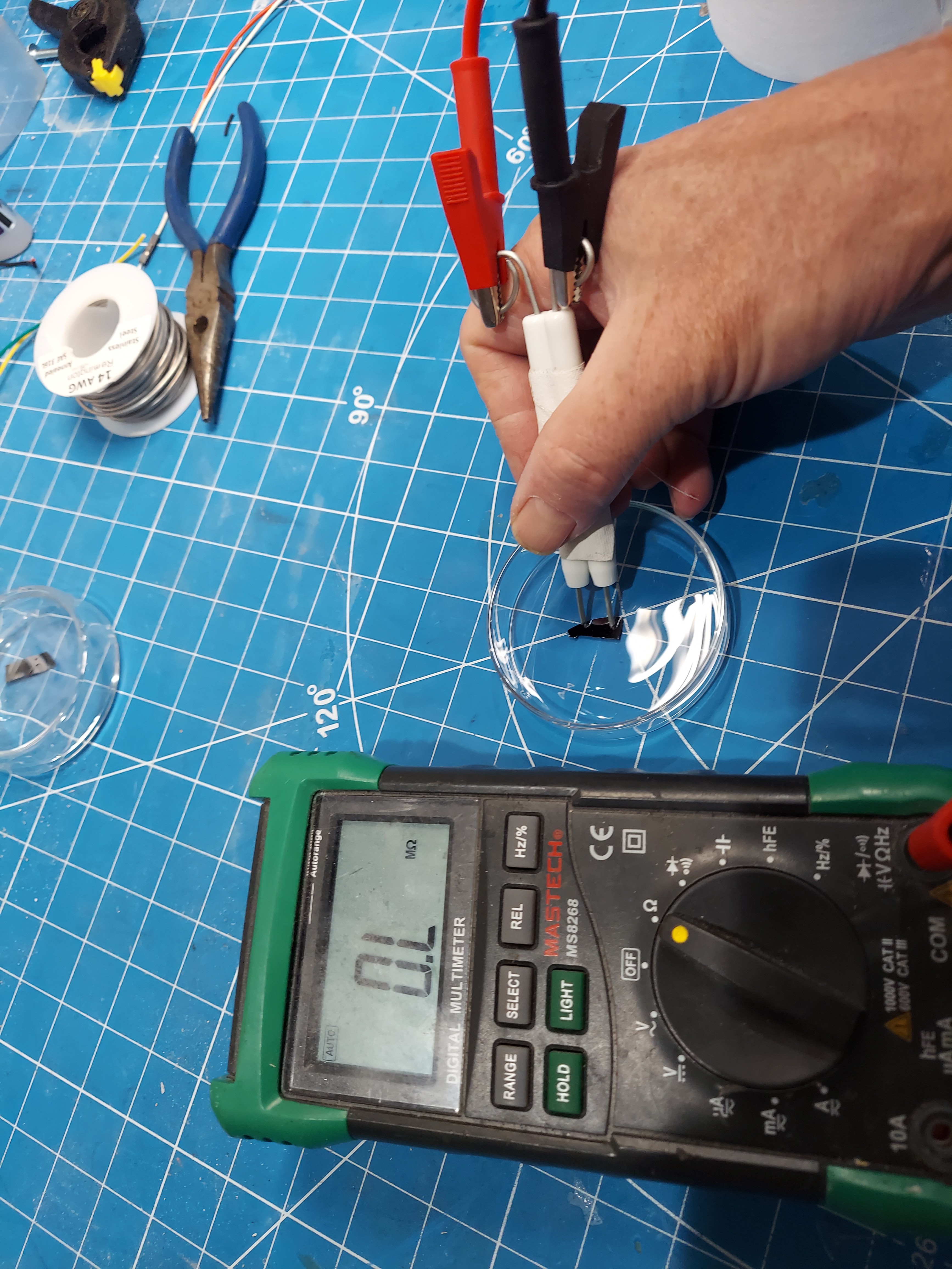
- I measured the resistance of the P-type wafer using a makeshift 1-cm probe after I received it. Oxide layers had already formed, so the results were difficult to determine - somewhere in the megaohms range.
- After a quick dip in some HF, the silicon was reading around ~300 KOhms/cm for the P-Wafer material.
- After doping the material with phosphorus, drying, and baking for 145 mins at 1000c, the material was retrieved, dipped in HF to remove the oxide layer, and retested. The material was now in the 30 -60 Ohm range per cm.
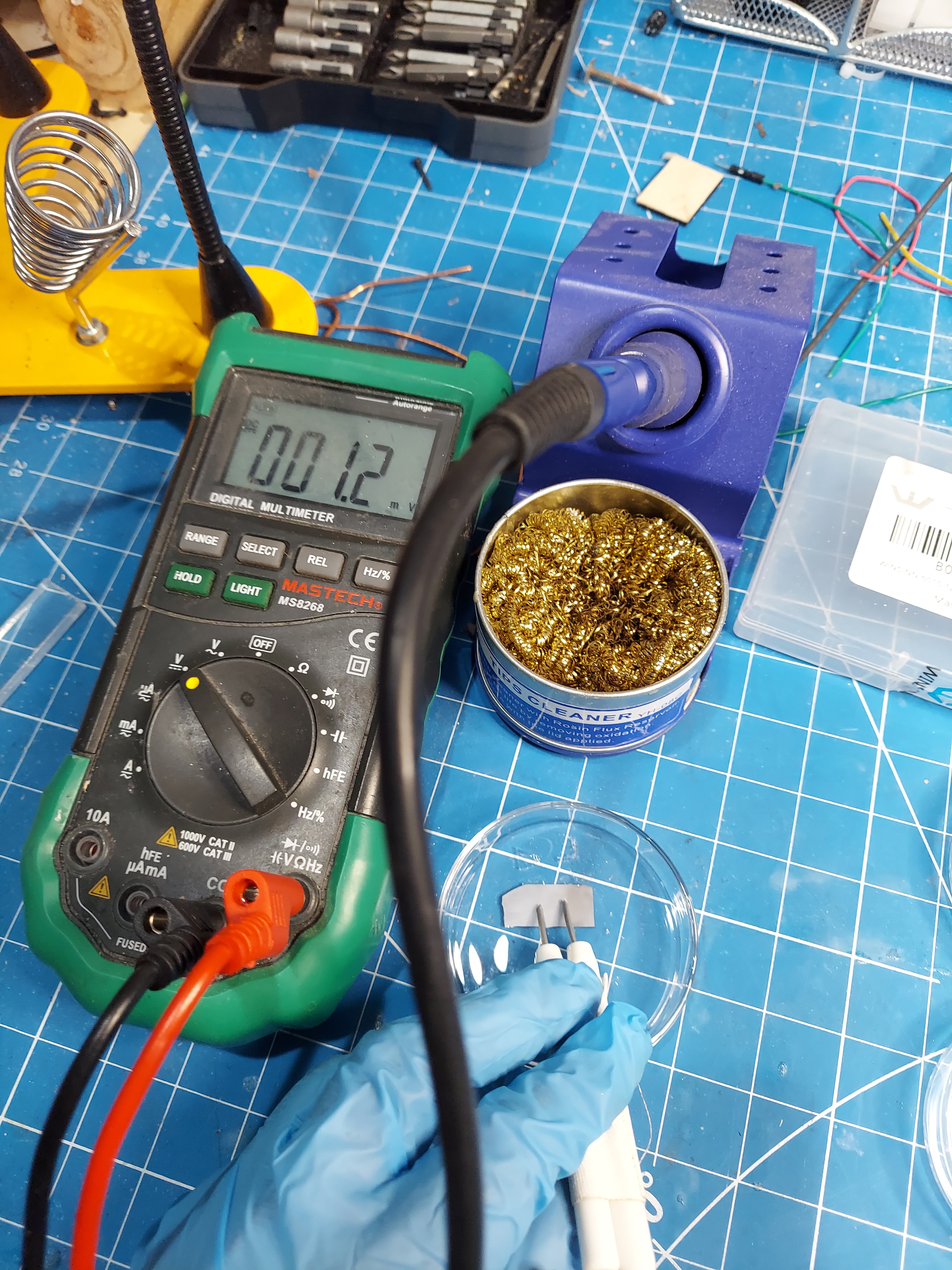
- The hot probe test on the positive anode also show the characteristic rise in voltage as heat was applied.
- This is a pretty good indicator that I was able to successfully dope regions of my p-type silicon with phosphorus, making it into an n-type material.
- I'm going to need a V/I curve tracer in order to better see how these semiconductors are behaving.
 Steve Hernandez
Discussions
Become a Hackaday.io Member
Create an account to leave a comment. Already have an account? Log In.