 Steve Hernandez
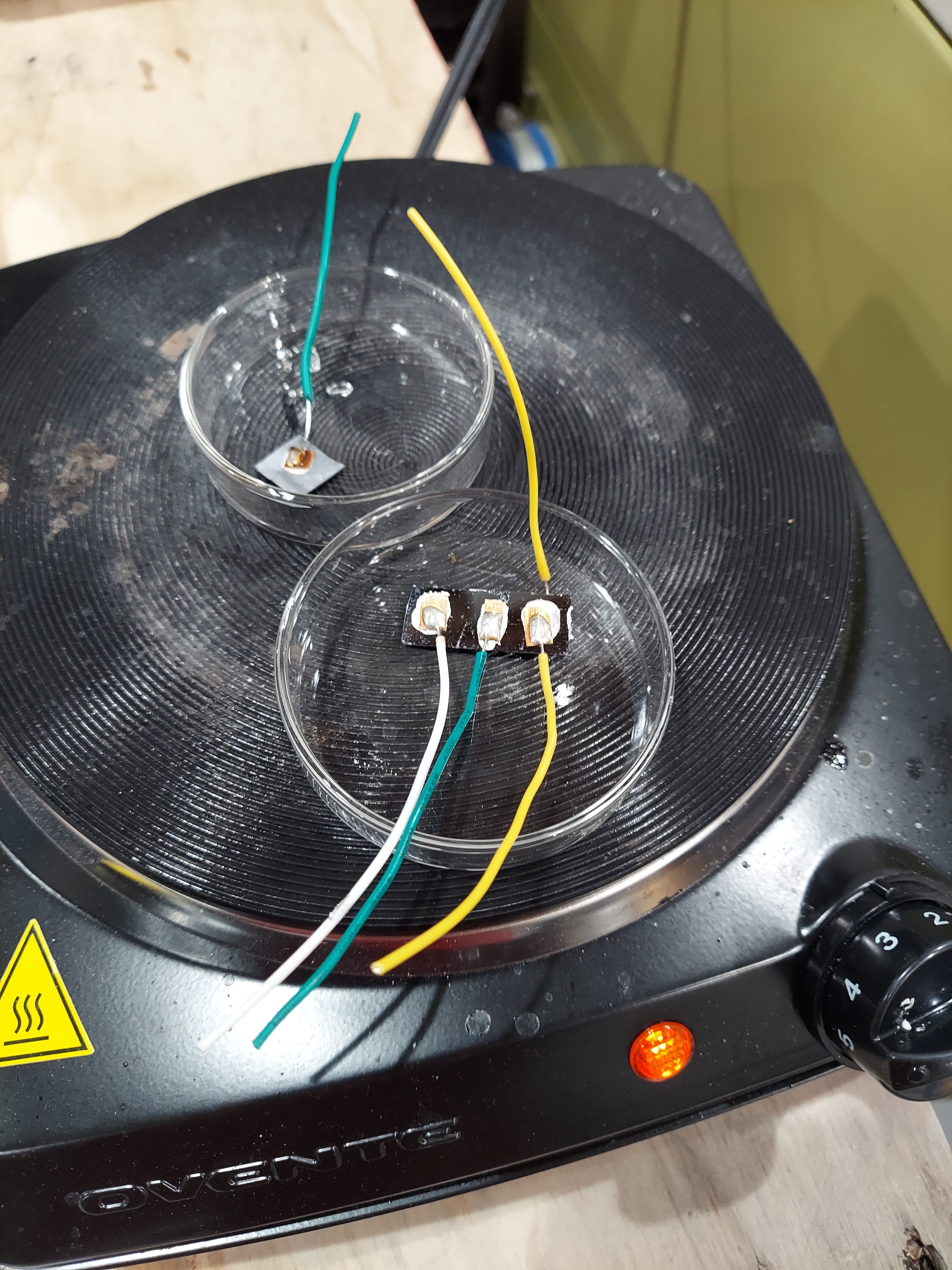
So after I got my Easy-Bake back in working order, I started experimenting with building actual devices. Previously - I worked though growing oxide layers, doping materials, masking, etching, and spin coating.
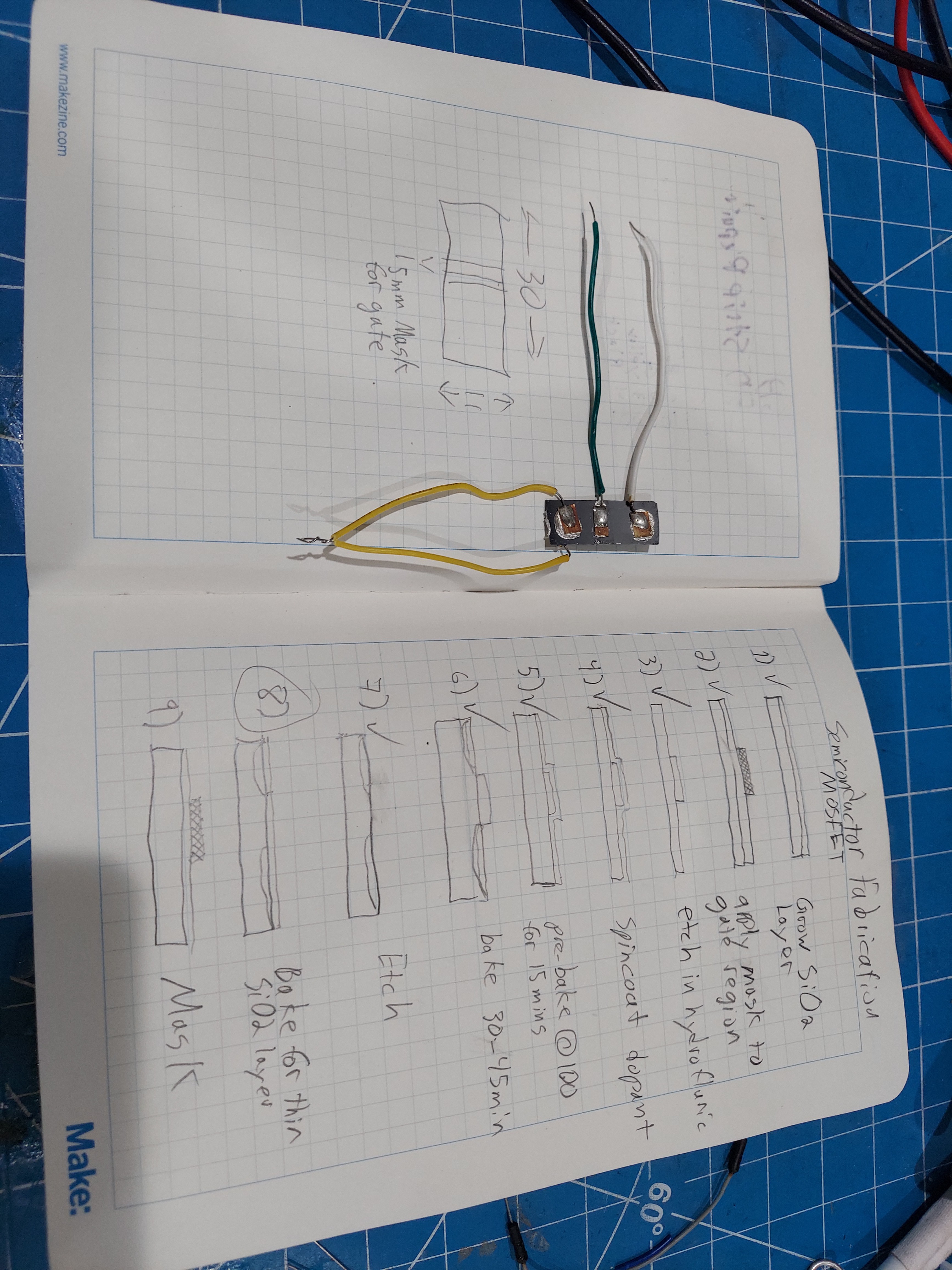
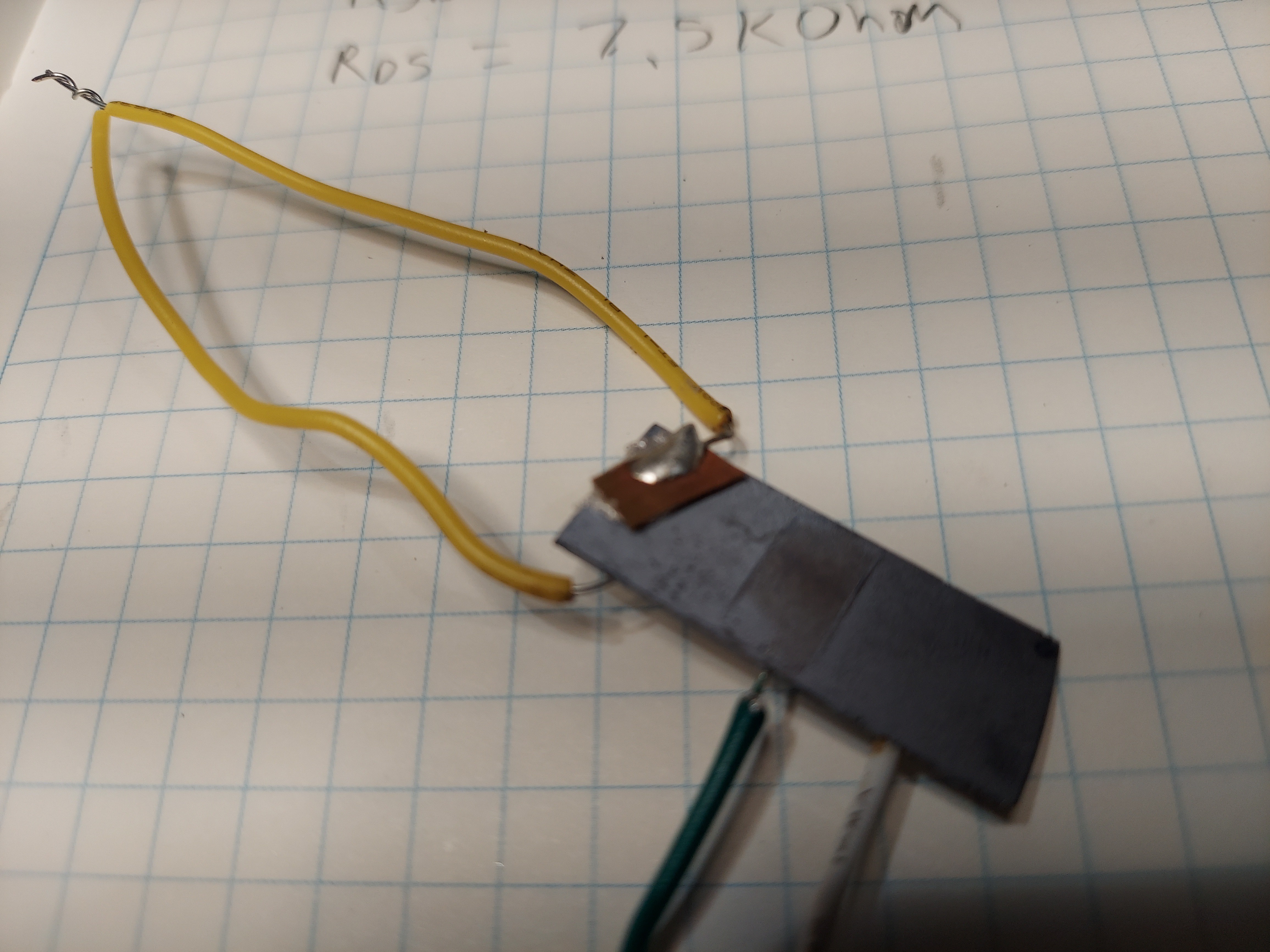
I decided to build a few simple PN junction devices - diodes. I also followed Sam Zeloof's recipe for a MOSFET - unfortunately - I'm fairly sure the gate shorted because the oxide was too thin.
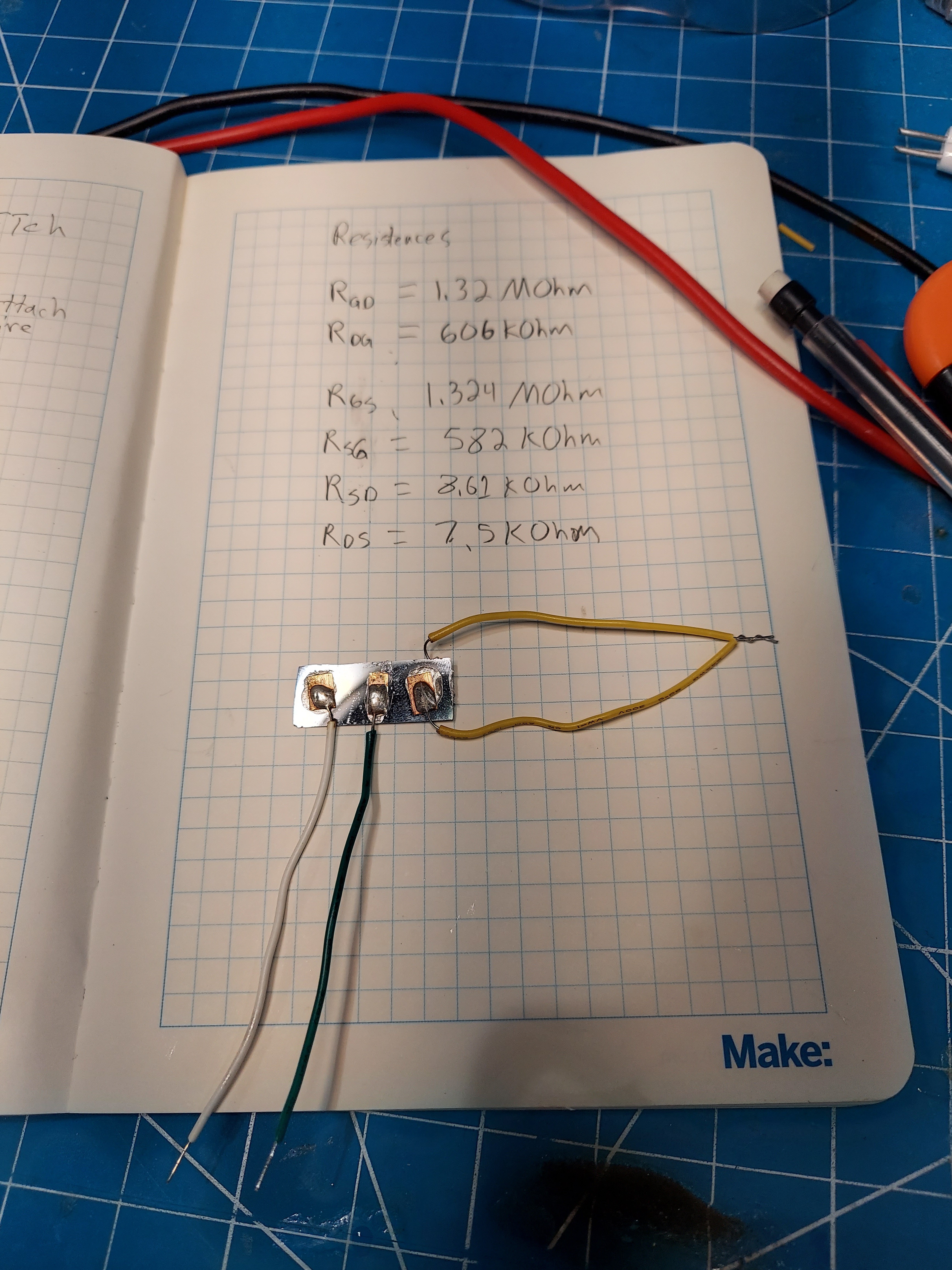
All the PN devices I built exhibited 'diode-like' properties - having a voltage drop higher in one direction, having a different resistance per direction. They also generated a small voltage under direct light.
I still need to buy or build a diode tester - aka 'octopus' device to generate V/I current traces.
It's been a steep learning curve the past week, and I think my devices are becoming more refined and successful.
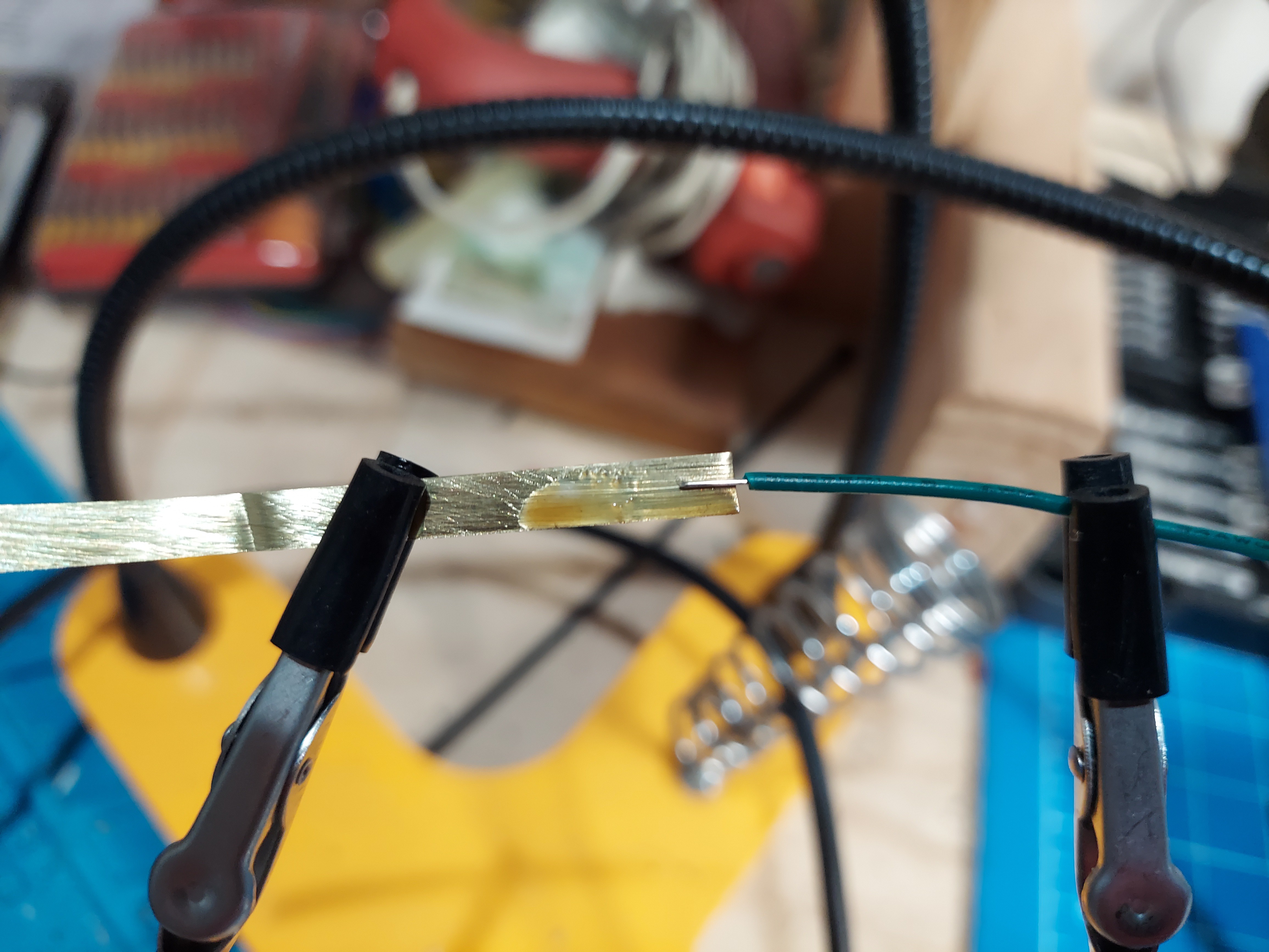
I'm making attachments to the silicon with small strips of sheet brass bonded with a silver epoxy. It's a heat-curing epoxy, not a 2-part epoxy, so it was more practical to have a footpad.
Discussions
Become a Hackaday.io Member
Create an account to leave a comment. Already have an account? Log In.