 mulcmu
Scanned board on scanner glass. Imported image into Fusion360 to scale and trace features. Exported DXF file to import into Kicad.
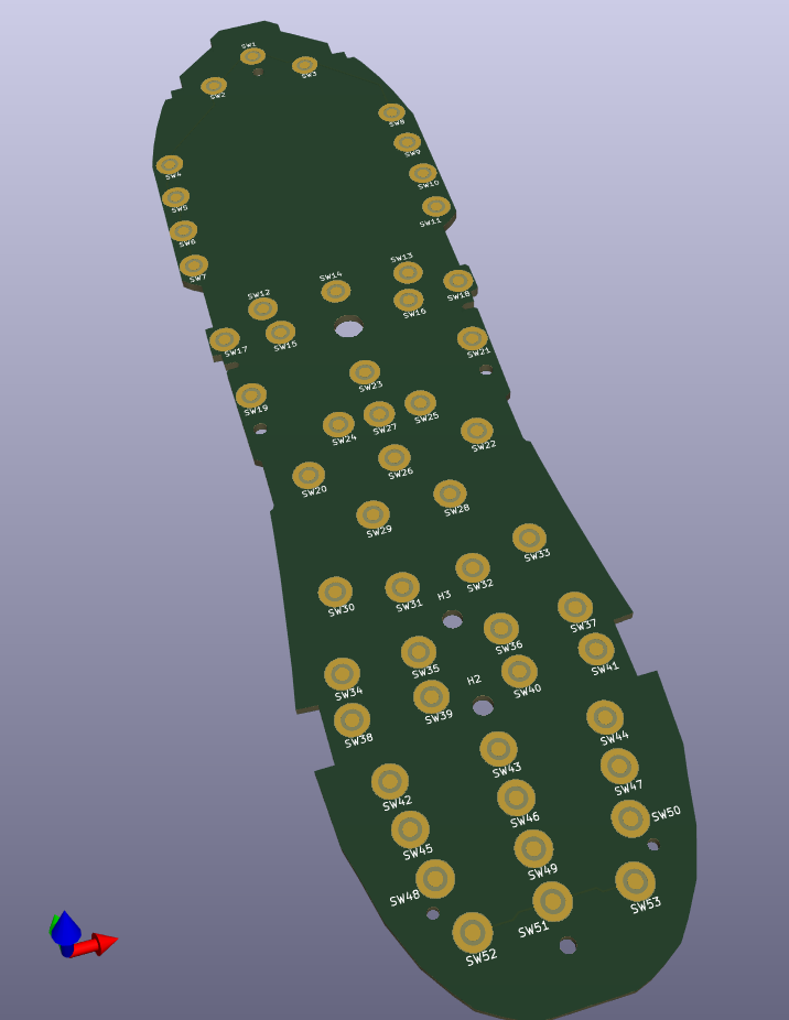
Factory PCB uses snap action dome contacts held in place with tape. Replicated same foot print. Kicad design has the button matrix and mounting holes so far.
TODO list for test fit PCB: Screen footprint, ESP32, MSP430, charging base connector, usb connector, battery connector.
Discussions
Become a Hackaday.io Member
Create an account to leave a comment. Already have an account? Log In.