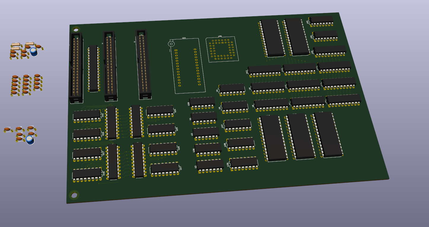
As I said in the last post, I wasn't happy with the multi-board format, so I've merged my Kicad schematics into one project and I'm going to do a new PCB. It should look roughly like this, measuring 225x150mm:

The PLCC part will be a dual UART (possibly a 68681?). Expansion cards can be plugged into the 40-pin IDC connectors. A couple of things are still missing, mainly a clock source and the address decoding logic.
This is my current plan for the memory map. It makes full use of the 64K SRAM and the 64K EEPROM, and provides another 64K of address space for expansion - leaving options open for a future graphics card. I'll use the UART's output port as the bank selection register, and it should only take a few extra gates to implement this.
|---------------| FFFF
|  I/O devices  |        256 bytes (32 bytes each for 8 I/O devices)
|---------------| FF00
|               |
|               |
|    48K RAM    |        Upper 48K of the 64K SRAM
|               |
|               |
|---------------| 4000   Banked area can be: lower 16K of RAM,
|    16K bank   |         any of the four 16K ROM pages,
|---------------| 0000    or any of the four 16K I/O pages
 kaimac
Discussions
Become a Hackaday.io Member
Create an account to leave a comment. Already have an account? Log In.
nice looking layout! look forward to seeing it assembled!
Are you sure? yes | no