 Guido
GuidoOverview
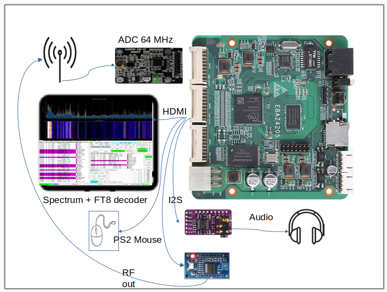
At the beginning the antenna is directly connected to the AD9226 Analog to digital converter, sampling at 64MHz. The 64MHz clock is generated by the FPGA, so that it can sample it well (more on this later)
Please note there's no external PC because the Zynq 7010 embeds a Dual Core Cortex A9 running Linux (Xilinx PetaLinux) in addition to its powerful FPGA.
- AM / SSB demodulated audio can be listened by headphone or loudspeaker
- Wideband or zoomed radio spectrum can be viewed on the screen
- demodulated FT8 can be viewed on screen and decoded using a WSJT-X adapted version
- modulated FT8 is sent to the Antenna
Similar projects
KiwiSDR is a very good example of a wideband 0-30 MHz FPGA based SDR receiver but it costs 450 Euro and it needs a BeagleBone computer.
Red Pitaya is a wonderful project with a lot of possibilities and it is open source but the board costs around 600 Euro.
Panoradio (https://panoradio-sdr.de/panoradio-sdr/) is much more than I'm trying to build (100 MHz spectrum, 16 bits samples) but its components (FPGA board, A/D board) are much more expensive as well.
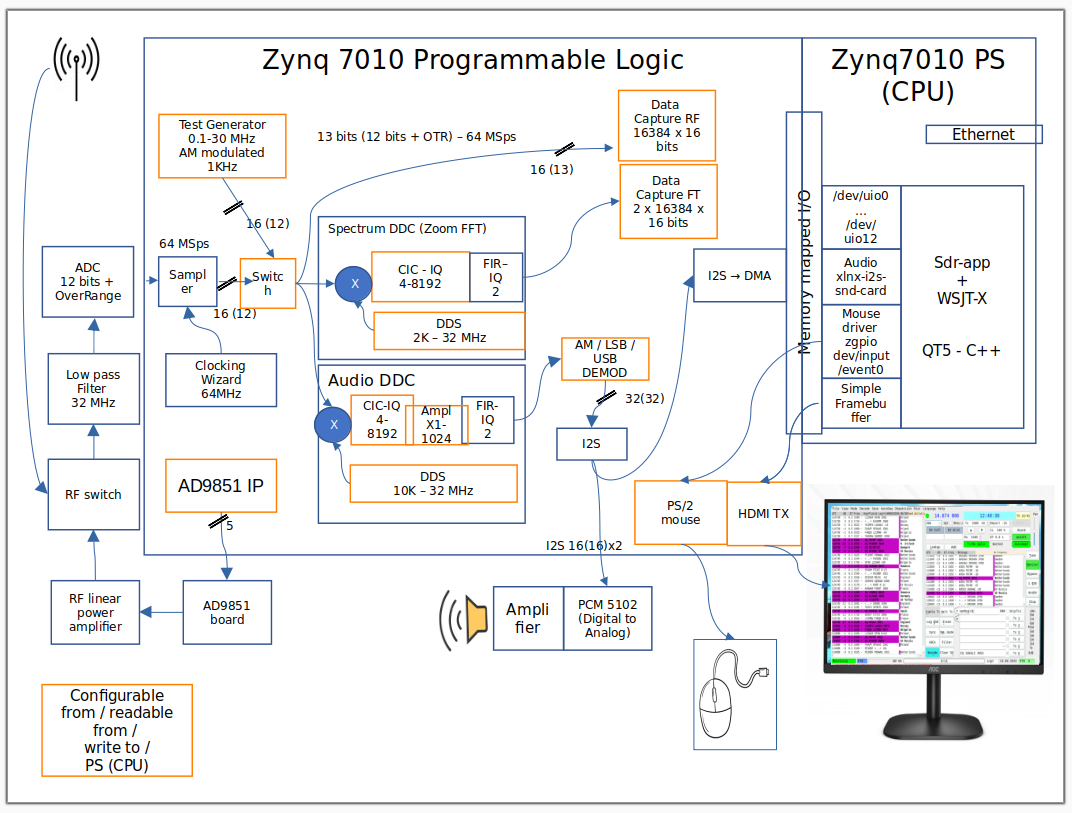
Block Diagram
At this time (Aug 2023) the whole design is pretty consolidated.
TODO:
- low pass 32 MHz
- RF Switch
- RF linear power amplifier
Numbers
All the number crunching in the fabric logic is perfomed with two's complement.
When I write xx(yy), e.g. 32(28), I mean that the numbers are 32 bit two's complement but the maximum expected value is
- 2^27 <= value <= 2^27-1
ADC - Analog to Digital Converter - AD9226
The board has no clock reference (see the AD9226 board schematic) and therefore the 64MHz clock must be supplied by the FPGA. In this way:
- the AD9226 outputs data on the dropping edge of the clock.
- the FPGA samples on the clock rising edge
See the picture below and for further details see the AD9226 datasheet from Analog Devices.
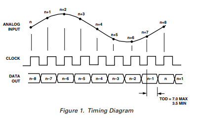
A concern is about the clock jitter coming from the FPGA. Will it add noise to the received signal?
For example, in this project ADC to DMA to Ethernet with a ZYNQ 7000, the sampling clock is generated outside the FPGA
FPGA
The functions operating in the FPGA are the following.
- It supplies a 64MHz clock to the AD9226 and receive 12 bit data + 1 bit "Over The Range" from it.
- An internal signal generator 0.1 - 30 MHz AM modulated at 1KHz can be be used for testing purposes.
- One "capture block" will capture 16384 samples (at 64MHz) at a time. These samples are sent to the FPGA PS and from there to the sdr-app (a QT5 C++ app running on the Zynq PS) to show the full 32 MHz radio spectrum and waterfall.
- One DDC (Digital Down Converters) with selectable bandwidth (10 MHz, 3 MHz, 1 MHz, 300KHz, 100 KHz, 30 KHz, 10 KHz,) will zoom the radio spectrum and waterfall with increased resolution.
- Another DDC can be tuned on a specific frequency to demodulate and decode e.g. the FT8 frequencies on 80 40 20 15 and 10 meters, with selectable (100KHz, 30KHz, 15KHz, 8KHz, 4KHz and 2KHz)
- It generates the TMDS signals to drive a DVI interface (HDMI without audio and control)
- It generates I2S signals to drive an external I2S DAC to listen to AM broadcasts and SSB radio hams
- It interfaces a PS2 mouse
Getting started with the EBAZ4205 board
The whole project is quite challenging, especially for those people who have never worked with Xilinx Zynq development environment (Vivado, Vitis, Petalinux). Therefore I strongly suggest to start with a "getting started" project. See my Hackaday project: EBAZ4205 development environment
The Analog Input
I didn't like that AD9226 12-BIT 65MSPS board attenuates the input signal by -8,4 dB. So I decided to modify it to get some amplification, using far more 12 bits ADC range.
I designed a circuit like this:
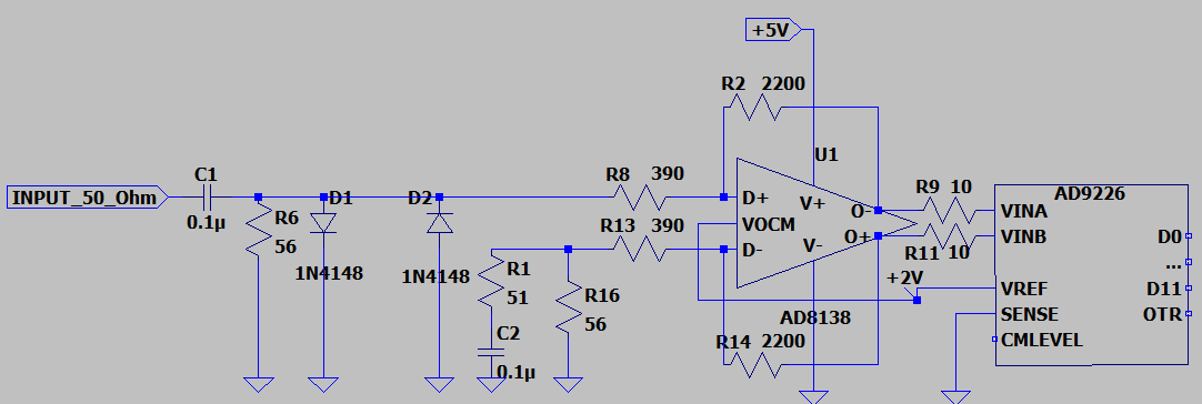
obtaining some 16,5 dB gain compared with -8,4 dB of the original circuit that was this one:
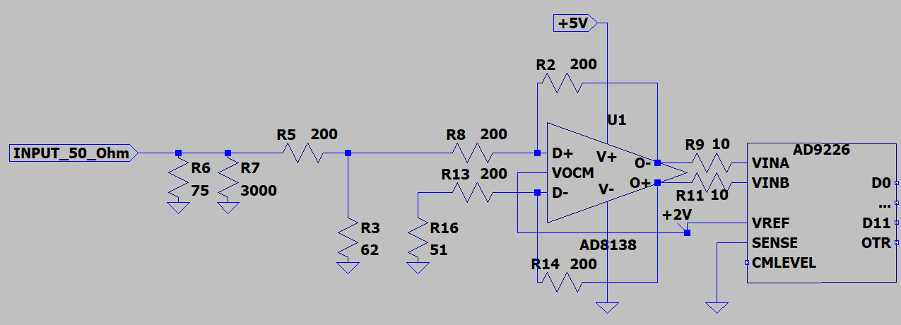
The modified board:
The Analog Input Dynamic Range
With the first stage amplification I set, the maximum input signal (the one generating 2 Vpp between VINA and VINB) is around -6 dBm.
Ethernet
The Ethernet port is connected to the local LAN, obtaining an IP address.
In this way, using an external PC, you can:
- launch one or more terminal sessions with SSH
- view the screen using a VNC server reading from the framebuffer (without X11)
- view / copy files via SFTP with FileZilla or similar
GUI
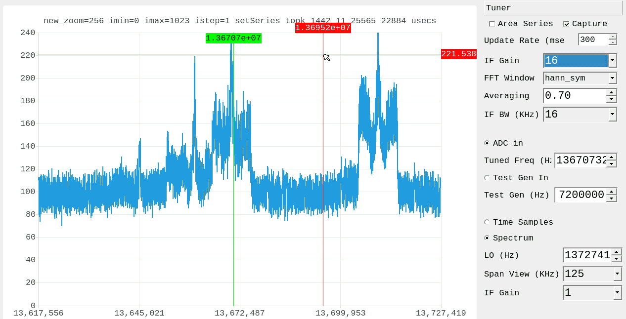
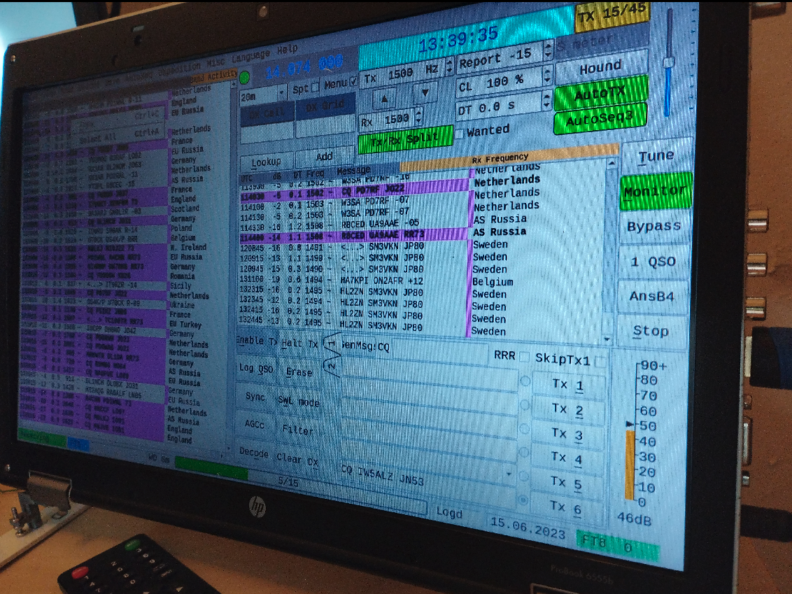
I decided to embed everything in the Zynq-7010, so I built a QT5 C++ application to view the spectrum and tune the radio stations. Its GUI appears like in the following pictures.
In this example, a 100 KHz wide spectrum where a radio station at 13,67 MHZ is tuned (see the vertical green line). Please note also the mouse point in red and the available settings on the right.
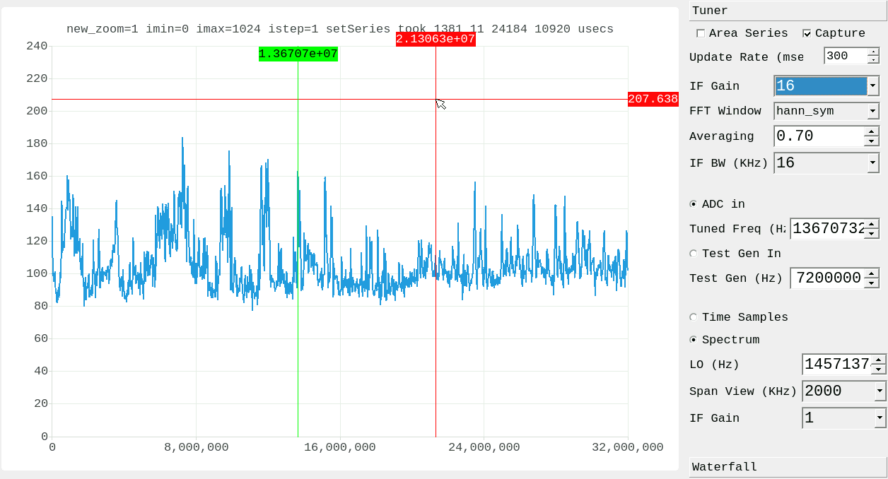
A 32 MHz wide spectrum where a radio station at 13,67 MHZ is tuned (the same as above).
RECEIVE SOME RADIO STATIONS AND HAMS
The solution implemented to display the spectrum by capturing sampled input burst can't obviously be used to receive radio stations, because:
- it receives some samples (16384) in a short time (256 usecs) with a frequency (around 100 - 200 Hz) depending upon the time (5-10 milliseconds) needed to build and display the spectrum, while to hear a radio station you need a continuos stream
- it would let the Processing System (i.e. the Zynq-7010 CPU) to do the heavylifting while the very powerful Zynq-7010 Programmable Logic would be under used.
Therefore I designed:
- a DDC (Digital Down Converter)
- a low pass CIC-FIR filters and decimators
- an AM / SSB / LSB demodulator
- an I2S interface
to listen to some audio at 48 Ksamples / second after getting it out the Zynq-7000 from.
32 MHz Low Pass Filter
(TODO)
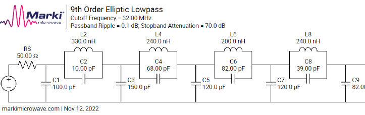
I need to attenuate the strong FM radios (88-108MHz) entering in the spectrum by the 3rd and 4th Nyquist zone and also some commercial repeater in the 2nd Nyquist zone. Hey! Don't you know much about Nyquist zones? Urgently read this: Nyquist Criterion and Sampled Data System Design.
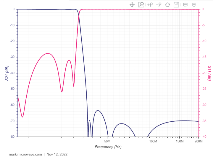
According to crun suggestions I should filter away the FM radio band (88-108) and also the AM band (up to 1,6 MHz). To filter the FM radios I thought to use an 9th order elliptic filter like this.
But I didn't do anything at the moment, because:
- before that, I'd like to receive and demodulate some short waves signals to understand the level of interferences;
- I intend to use the Out of The Range bit from the ADC to diagnose if a strong signal is intermodulating my reception forcing the ADC to go out of the 12 bits range.
DDC (Digital Down Converter)
As usual, It is composed by a Local Oscillator and a Complex Multiplier.
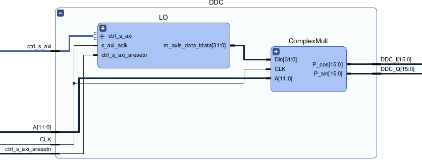
Note that the Local Oscillator, its AXI Control and the Complex Mutliplier all use a 64 MHz clock (CLK).
Local Oscillator
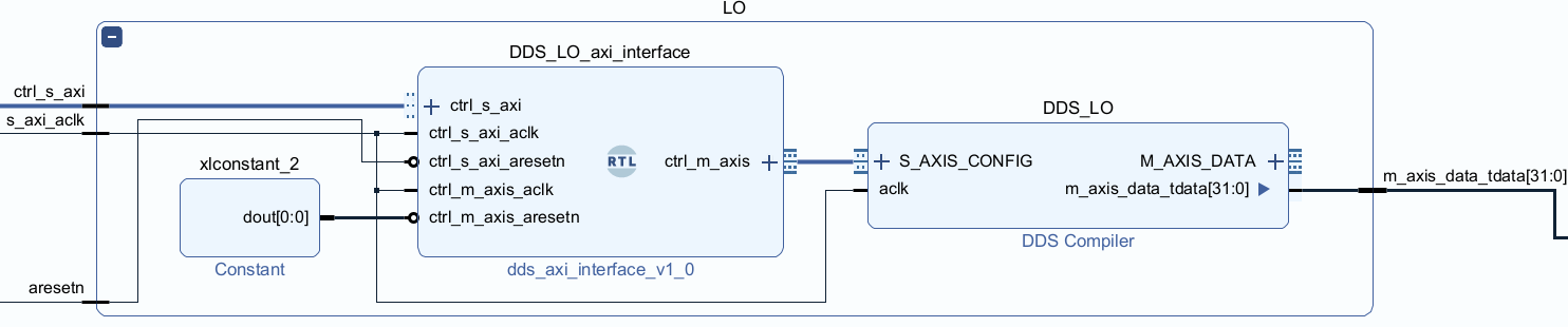
- It outputs a 32 bits complex (16 bits sine + 16 bits cosine) signal
- Its frequency is set by an usual ctrl AXi interface.
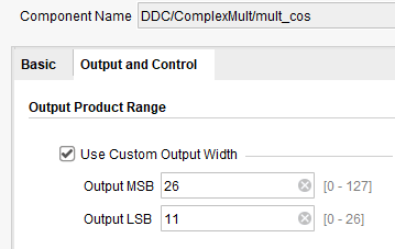
Complex Multiplier
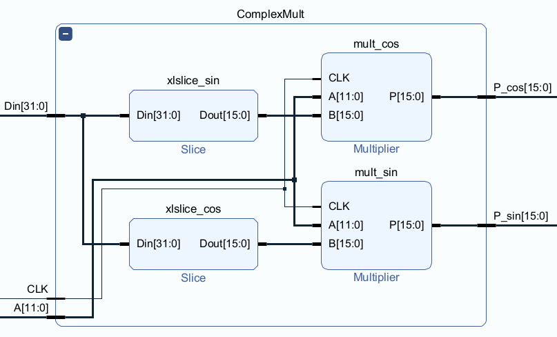
- The 32 bits complex (16 bits sine + 16 bits cosine) signal is split into two 16 bits signals
- The 12 bits by 16 bits multiplication (28 bits) is truncated to the first 16 MSBs.
Test Signal Generator
To test the fabric logic and the whole design even without an external signal and without involving the ADC, I rapidly understood the need of an internal test signal. Using a Xilinx DDS compiler IP I designed the following block:
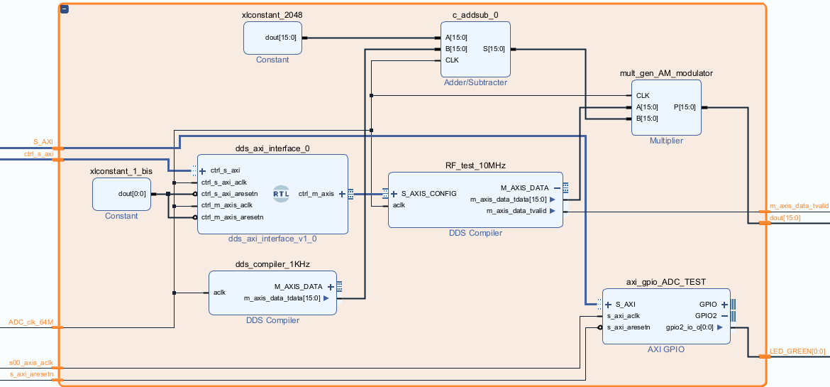
It produces a carrier AM modulated with 1 KHz tone. The carrier frequency can be set from 0 to 32 MHz (and beyond in necessary).
CIC-FIR
I found two very well explained articles:
- A Beginner's Guide To Cascaded Integrator-Comb (CIC) Filters
- Intel - Altera: Understanding CICO Compensation Filters
Main Facts about CIC-FIR
The standard configuration is to design one or two programmable consecutive CIC filters/decimators, followed by a fixed FIR filter.
about CIC:
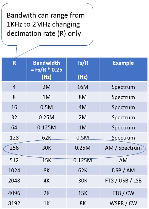
- the number of stages is fixed (N=8)
- the R decimation rate allows to set the overall CIC+FIR filter bandwith.
- In my design R=4...8192 spans bandwith between 2MHz and 1 KHz (see the table below).
about FIR:
- very sharp transition bandwith (e.g. -3dB at 2MHz and -120dB at 2,42MHz)
- very high stopband attenuation (-120dB)
- compensation of the CIC filter mild drop
- it is obtained using a 110 coefficients FIR filter, calculated with matlab:
- It furtherly decimates by two to halve its complexity (half DSP48 used). For details see A Beginner's Guide To Cascaded Integrator-Comb (CIC) Filters
While testing my CIC-FIR dual channel solution I met a problem I submitted to the Xilinx/AMD support.
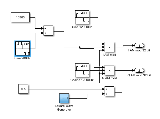
AM Demodulator
I essentially copied the design by K6JCA - An FPGA SDR HF Transceiver
AM demodulator
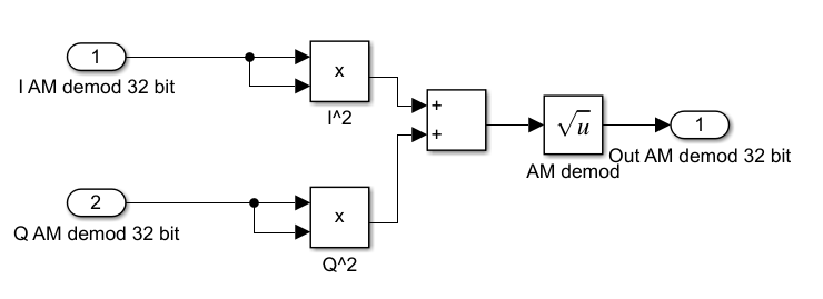
It is a classical envelope detector performing sqrt ( I^2 + Q^2 ) .
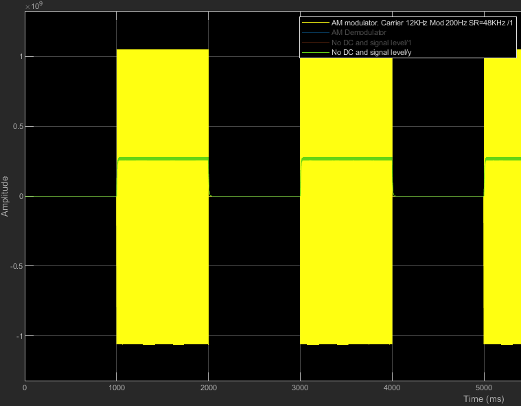
See below in yellow a test signal (the I component only) entering this AM demodulator and in blue the AM demodulated.
No DC and signal level meter
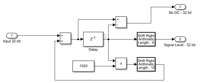
To remove the DC component from the AM demodulated, I simply used a first order IIR highpass filter, which can also give the carrier level obtained low passing the AM demodulated signal.
See below in red the AM demodulated and with the DC component removed by the high pass IIR filter. In green the carrier level.
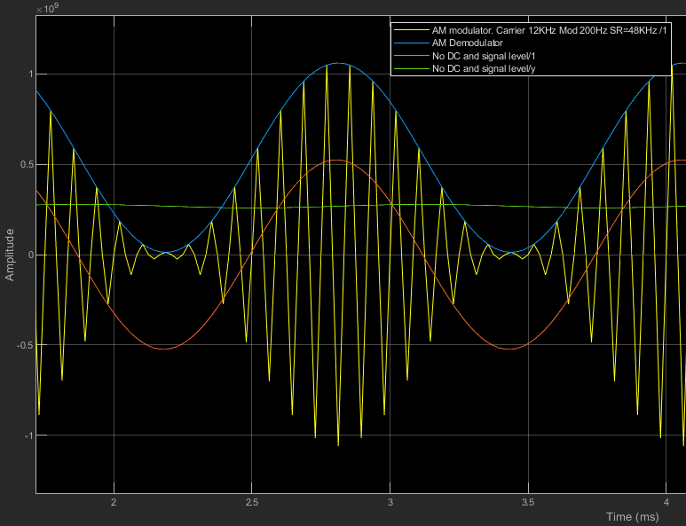
This is the complete testbench I used in Simulink.
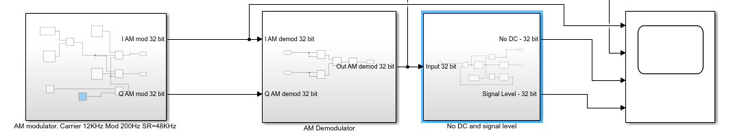
Beside the AM demodulator and the high/low pass filter, note the test signal I used (leftmost block). It is designed to produce a 1 second AM modulated signal followed by 1 second without any signal, to test the transient response of the signal level meter.
This is its block diagram
and its output (I component only) in yellow.
In green you can see the signal level meter response.
AGC
Designed and simulated but not tested yet
It acts after AM / SSB demodulation.
It is the kind of Automatic Gain Control called "forward" i.e. it adjusts the output level without reaction on previous stages but simply amplifying / attenuating the signal itself.
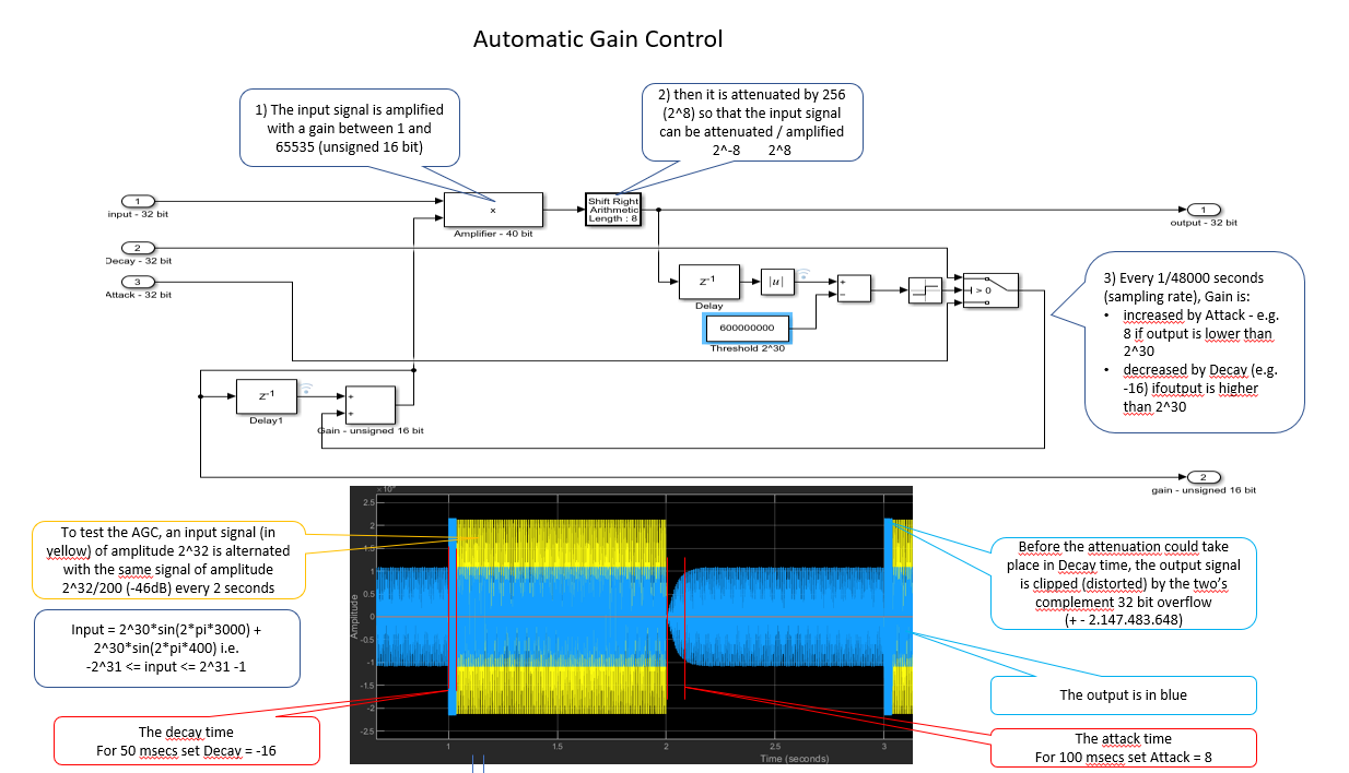
Simulated with Simulink and converted to VHDL.
I2S Test
I decided to use I2S to get audio out from the Zynq. To better understand the reasons, see the log.
To test the IP (I2S_Transmitter) and the I2S DAC (PCM5102) I built this Vivado block:
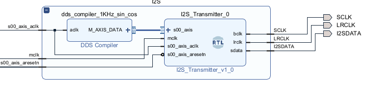
A few facts:
- The dds_compiler generates a 16 bits two's complement sine and 16 bits cosine at 1 KHz (sampled ad 100MHz as the AXI stream clock s00_axis_aclk)
- The I2S_Transmitter IP comes from http://www.harald-rosenfeldt.de/2017/12/30/zynq-create-an-i2s-transmitter-to-send-audio-signals/
- SCLK, LRCLK and I2SDATA are the standard I2S wires.
- mclk=10MHz and consequently:
- SCLK = 1.536MHz (see I2S_Transmitter.v)
- the audio sampling rate (LRCLK) is 1.536MHz/32 (16+16bits) = 48.000 Hz
This is the I2S data protocol:
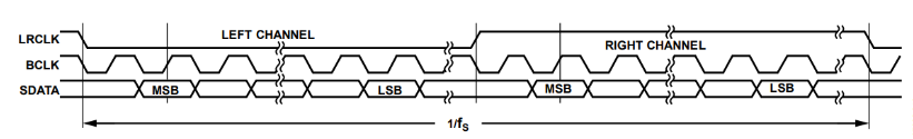
BCLK is SCLK SDATA is I2SDATA fs = 48.000 Hz
DAC (PCM5102) and class D audio amplifier (PAM8403) schematic.
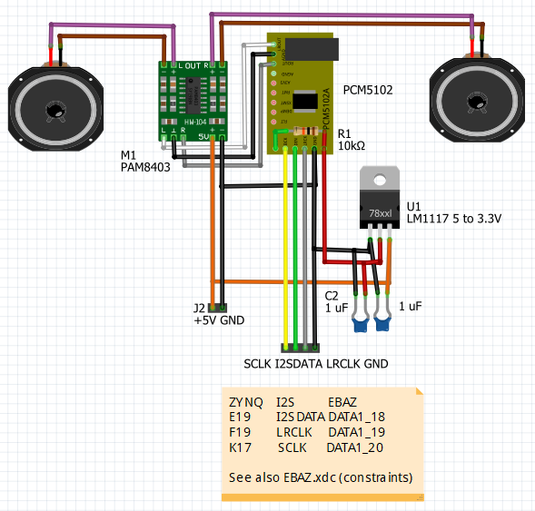
Please note:
- the Linear Regulator 5 to 3,3V (PCM5102 cannot stand 5V)
- there's no need for the stereo output but the two channels can be useful for different purposes:
- one channel for LSB audio and the the other one for FT8 audio
- one channel for I data and the other one for Q data (before demodulation)
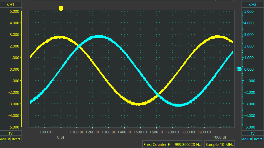
And finally these are the left and right outputs.
WSJT-X / JTDX
It runs inside the Zynq PS as a normal Linux program to decode FT8 or other digital mode. See the GitHub project for details.
Of course the JTDX program must be supplied with an audio input. See the next paragraph.
Audio output (from PL to PS)
As you can see in the block diagram, the output of the I2S transmitter goes out to the I2S (DAC) decoder but it also goes to a "I2S to DMA" block by which the audio samples are copied to a memory mapped area via DMA and collected from the "Xilinx I2S audio Linux driver".
Zoom FFT Receiver
I copied the idea from Panoradio (https://panoradio-sdr.de/panoradio-sdr/).
In fact if you need to view the spectrum details of modulated signals, you need to zoom the spectrum collecting a sub band of it.
E.g. 8192 time samples of a 0-32MHz spectrum let's you to view the spectrum with a "definition" (frequency bin span) of 32M/8192 = 3906,25 Hz which means you see the full FT8 7,074 MHz band in a single bin .
For this reason I built such a separate receiver (DDC + IF Filter + AXI Capture) to get the RF spectrum of a desired sub band with the wanted definition. See Spectrum DDC (Zoom FFT) in the block diagram at the beginning of these "details".
SSB Demodulator
The obvious choice is to build a Weaver demodulator, very well described here Weaver SSB Modulation/Demodulation - A Tutorial by Derek Rowell.
You should also read the original article by Donald Weaver A Third Method of Generation and Detection of Single-Sideband Signals," Weaver, Proceedings of the IRE, Dec., 1956
This is my design.
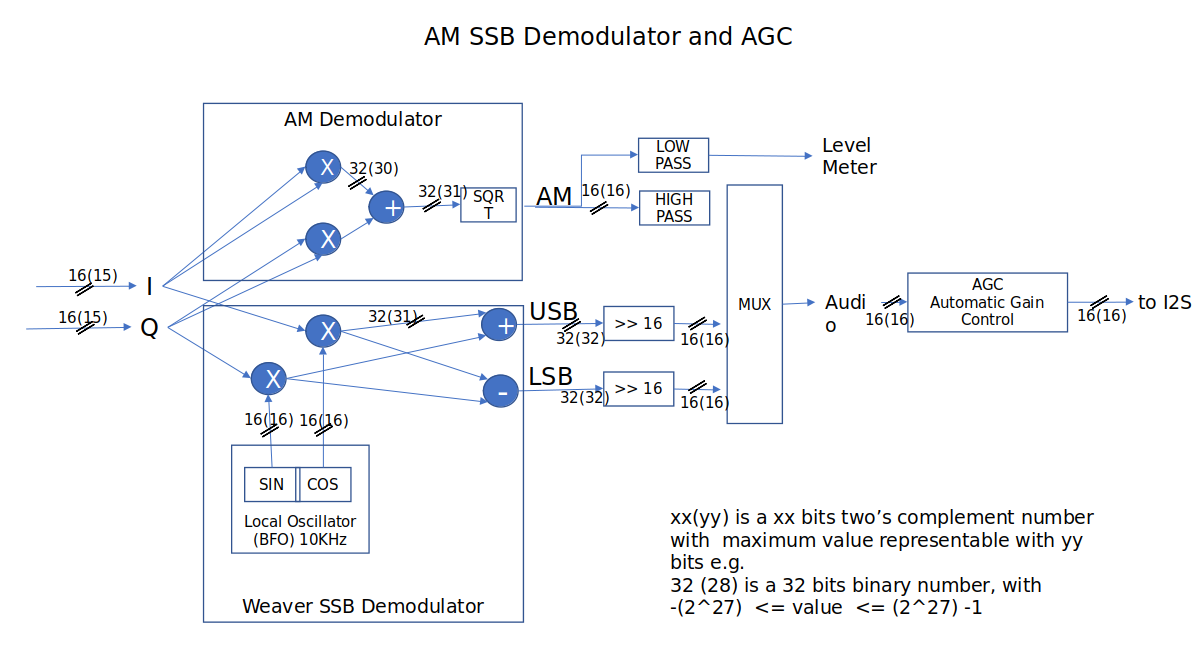
Of course the frequency of the BFO must be set at the boundary of the IF low pass filter, as described in the article.
Summary:
To demodulate an USB signal with frequency ωc (carrier frequency) using a low-pass filter
with cut-off frequency ωo,
- Set the tuning oscillator to the frequency ωs = ωc + ωo,
- Select the audio output as the sum = I x cosωot + Q x sinωot
To demodulate an LSB signal with frequency ωc (carrier frequency) using a low-pass filter with cut-off frequency ωo,
- Set the tuning oscillator to the frequency ωs = ωc - ωo,
- Select the audio output as the difference = I x cosωot - Q x sinωot
where:
- ωs = local oscillator frequency
- ωo = BFO frequency
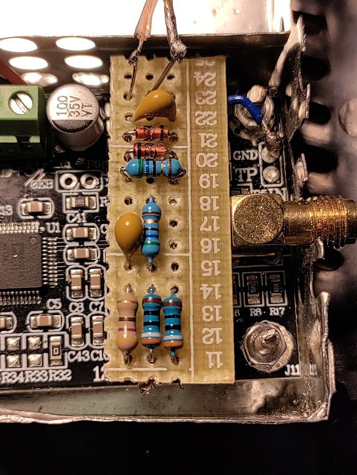
My Assembly
I placed all the boards in a plastic box scavenged from an old modem.
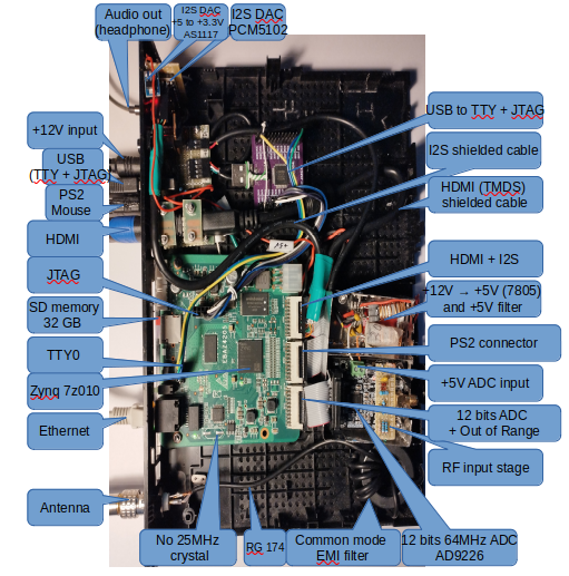
Even the HDMI screen (Samsung 1366 x 768 LCD) was scavenged from an old HP laptop and adapted to HDMI using an HDMI to LVDS interface board (10 $)
FT8 QSO's
Now that the whole project works pretty well as a receiver, including FT8 decoding, it's time to transmit anything. To know something about the FT8 protocol, see FT4_FT8 and my resume in the log.
MYJTDX software (forked from JTDX forked from WSJT-X) decodes well and it is ready to transmit and manage QSO's.
I decided (see the log for details) to use an external DDS, programming its output frequency to:
- modulate 8FSK
- modulate its amplitude to generate the ramps (raised cosine initial amplitude increase and final amplitude decrease) of FT8. See "FT8 Ramp up and down" below.
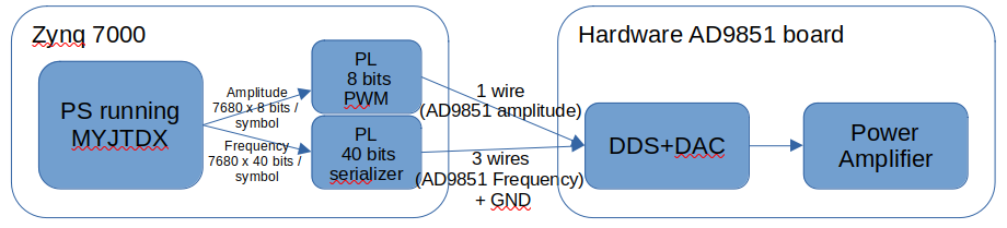
See the AD9851 DDS datasheet and the AD9851 (DDS + DAC) board I used.
Zynq-7010 - AD9851 Wirings
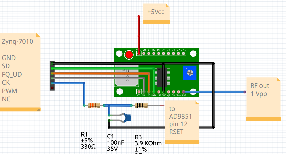
Note the RC low pass filter (R1-C1) to get a DC level from the PWM 2 MHz waveform. If it is not enough attenuating 2 MHz, I'll change it with an LC multiple poles low pass filter.
FT8 Gaussian Frequency Shift Keying Transmitter
My second attempt to get the FT8 messages out from the myjtdx linux app and send them to the external DDS (AD9851 board) succeeded!
For those of you interested in undestanding the first unsuccessful attempt, it is documented in this log Vivado AD9851 first attempt.
For this final solution a home made IP component written in VHDL (PL GFSK in the following picture) receives via AXI4-Lite the 79 symbols (each symbol is 3 bits each) composing the FT8 message. In this way the Linux software (MYJTDX) and the Cortex A9 CPU have plenty of time to send these 10 x 32 bits every 15 seconds. Besides, the carrier frequency (e.g. 7075500 Hz) must be sent to the AD9851 because the user can choose it by the MYJTDX user interface..
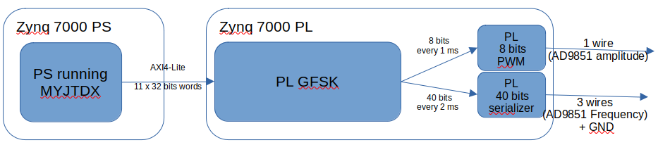
Therefore the message from PS to PL is composed by the following 11 x 32 bits words.
MSB LSB
- R0 : Phase shift for the carrier frequency (when symbol value=0): 32 bits
- R1 : Symbol 8 (4 bits) Symbol 7 (4 bits) ... Symbol 1 (4 bits)
- ...
- R10 : Symbol 73 (4 bits) ..... Symbol 79 (4 bits) 0000
NOTE Please note that an FT8 symbol (0...7) could be encoded with 3 bits but for AXI4-Lite convenience (8 bits alignment) I decided to encode a symbol in 4 bits leaving the MSB at 0.
As I already built the AD9851 PWM and AD9851 serializer, it's now time to design the GFSK IP.
FT8 Ramp up and down - VHDL implementation
According to the FT8 protocol, the first and last symbols amplitude shall follow a ramp up and a ramp down.
The IP component I designed generates a DC signal (averaging a 2MHz PWM) to amplitude modulate the AD9851.
For details about AD9851 Amplitude Modulation see this
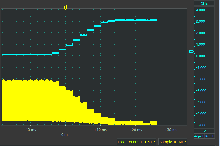
See the result for 20 miliseconds ramp down in the following picture, where you can see the blue voltage:
- 0 Volts=max amplitude
- 3.3 Volts= minimum (no amplitude)
and the corresponding signal (DAC output) amplitude in yellow.
The raised cosine ramp down values are obtained by the following array of constant values
constant rampup : rampup_type := (0,0,0,0,0,2,14,37,70,108); -- 20 msecs ramp up
used in this way:
- sample_ndx = 0 ... 9th rampup(sample_ndx)
- sample_ndx = 10 ... 19th 255 - rampup(19-sample_ndx)
FT8 Samples and Symbols - VHDL impementation
When the 11 registers described in "FT8 Gaussian Frequency Shift Keying Transmitter" are loaded, the VHDL code start counting the 81 symbols (sym_counter increases every 160 milliseconds) and, in an inner loop, 80 samples (sample counter increases every 2 milliseconds).
See the following main process which sets the values of:
- pwm_dc: an 8 bits number to amplitude modulate the output of AD9851
- data_out_t: a 32 bits number representing the phase shift of each sample
every 2 milliseconds
process( read_data_out_t ) is
begin
  -- 149 is 6.25Hz * 2^32 /180MHz
  -- phi_out <=  std_logic_vector ( b"00000001" & to_unsigned(  to_integer(unsigned(phi0)) +  149 * to_integer(unsigned(data_out_t)) / 1024, 32 ));
  phi_out <=  std_logic_vector ( unsigned(ad9851_ctrl) & to_unsigned(  to_integer(unsigned(phi0)) +  149 * to_integer(unsigned(data_out_t)) / 1024, 32 ));
  -- data_out <= data_out_t;
  if (rising_edge (read_data_out_t)) then
    if ( S_AXI_ARESETN = '0' ) then
       sym_counter <= 0;
       sample_counter <= 0;
       pwm_dc <= x"FF";
       last_msg <= msg_counter;               -- this msg is completely sent to AD9851
    elsif  sample_counter < 79 then           -- 80 samples per symbol
       sample_counter <= sample_counter + 1;

       -------------------------------------------------------------------------------------------------
       -- build the values of data out_t and pwm_dc for sym_counter (0,80) and sample_counter(0,79)
       if(sym_counter = 0) then
           if(sample_counter < 10) then
               ad9851_ctrl <= b"00000001"; -- AD9851 power on
               pwm_dc <= std_logic_vector( to_UNSIGNED((255-rampup(sample_counter))*pwm_divider/255,8));  -- first half ramp from 0 to 102
               data_out_t <= std_logic_vector( UNSIGNED(symbols(0)) * TO_UNSIGNED(1024 , 29));
           elsif(sample_counter < 20) then
               pwm_dc <= std_logic_vector( TO_UNSIGNED ((rampup(19-sample_counter))*pwm_divider/255,8)); -- second half ramp from 154 (256-102) to 255 (256-0)
               data_out_t <= std_logic_vector( UNSIGNED(symbols(0)) * TO_UNSIGNED(1024 , 29));
           else
               data_out_t <= std_logic_vector( UNSIGNED(symbols(0)) * TO_UNSIGNED(1024 , 29));
           end if;
       elsif(sym_counter < 80) then
           -- sym_counter = 1 ... 79
           if(sample_counter < 19) then
               data_out_t <= std_logic_vector(
                       UNSIGNED(symbols(sym_counter-1)) * TO_UNSIGNED(1024-pulse(18-sample_counter), 29) +
                           UNSIGNED(symbols(sym_counter  )) * TO_UNSIGNED(pulse(18-sample_counter)     , 29)
               );
           elsif sample_counter<60 then
               --- 19 <= sample_counter < 60
               data_out_t <= std_logic_vector(
                           UNSIGNED(symbols(sym_counter  )) * TO_UNSIGNED(1024                     , 29)
               );
           else
               --- 60 <= sample_counter < 80
               data_out_t <= std_logic_vector(
                       UNSIGNED(symbols(sym_counter  )) * TO_UNSIGNED(pulse(sample_counter-60)     , 29) +
                       UNSIGNED(symbols(sym_counter+1)) * TO_UNSIGNED(1024-pulse(sample_counter-60), 29)
               );
           end if;
       else
           -- sym_counter = 80
           data_out_t <= std_logic_vector( UNSIGNED(symbols(80)) * TO_UNSIGNED(1024 , 29));

       if(sample_counter >= 60 and sample_counter < 70) then
           -- ramp down first half
           pwm_dc <= std_logic_vector( to_UNSIGNED(rampup(sample_counter-60)*pwm_divider/255,8));  -- first half ramp from 0 to 102
       elsif(sample_counter >= 70 and sample_counter < 80) then
           -- ramp down second half
           pwm_dc <= std_logic_vector( TO_UNSIGNED ((255-rampup(79-sample_counter))*pwm_divider/255,8)); -- second half ramp from 154 (256-102) to 255 (256-0)
       end if;
        end if;
    -- end of build the value of data out for sym_counter (0,80) and sample_counter(0,79)
    -------------------------------------------------------------------------------------------------
    else
        -- sample counter reached 80 -> reset it to 0
        sample_counter <= 0;
        if sym_counter = 80 then
             sym_counter <= 0;
             last_msg <= msg_counter; -- this msg is completely sent to AD9851
             ad9851_ctrl <= b"00000101"; -- AD9851 power off

        else
             sym_counter <= sym_counter + 1;
        end if;

    end if;  -- end if sample_counter
  end if;    -- end if rising edge
end process;
You can see the full VHDL source code of AD9851_gfsk on my Github repository.