 kaimac
Here is what I am thinking of for the "ALU":
- We need a way to load the accumulator with an immediate value ("lda 3"), or from a memory location ("lda $3"), so a mux is required there.
- At a minimum we want to be able to add a value to the accumulator. We already have that mux so the value could be immediate or direct. Another mux is needed to select between "add" and "load". The input port can also feed into that mux.
- At the cost of one extra chip, a logic function will be very useful. I've put NOR in the diagram but after playing around I think NAND is slightly more useful (easier to do AND for testing bits).
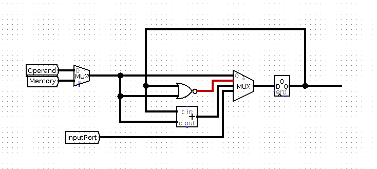
That allows for these instructions:
000m vvvv  lda    acc = value
001m vvvv  add    acc = acc + value
010m vvvv  nan    acc = ~(acc & value)
011x xxxx  in     acc = in

m: 0=immediate value, 1=value from given RAM address
v: 4-bit value
x: don't care
I really like how this turned out, because the decoding for these instructions requires no additional chips!
opcode bits:
   3210 vvvv
   ||||
   |||\- operand/memory mux select
   ||\-- accumulator source mux select
   |\---             -"-
   \---- accumulator write enable (active low)
Two opcodes are taken up by "in" but it's worth that small cost.
Discussions
Become a Hackaday.io Member
Create an account to leave a comment. Already have an account? Log In.