 micl
micl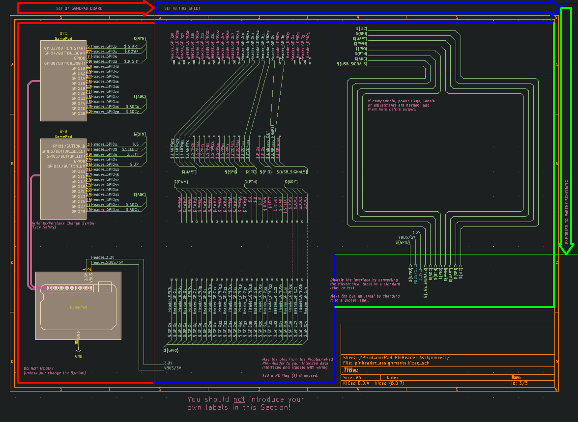
I'm not sure how familiar the general public is with hierarchical schematics in KiCAD, but they're powerful if you use them the right way. To make these boards easy to extend, the way that students design extensions for them should be clean.
On the outside of the schematic which abstracts the hardware mappings, you refer to the datasheet listed titles for functions of the RP2040, and while in the firmware you would need to address the correct mappings of pin-to-interface, this makes it possible to work with the final pin functions.
At the end of the day, if both two pins (i.e GPIO4 and GPIO10) are used for function A or B, and both _can_ perform A *OR* B, then the order does not matter. Instead, in the parent schematic, all you see is:
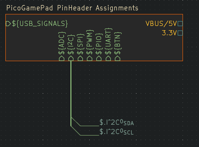
And you simply connect the pin for X to the thing that needs X. For example:
Discussions
Become a Hackaday.io Member
Create an account to leave a comment. Already have an account? Log In.