 micl
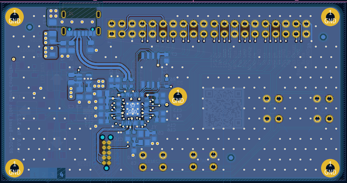
miclThe first version of the board (pictured below) was made to satisfy JLCPCB's tighter standard 4-layer via tolerances. This turned out to be an issue, and there were a few other reasons I moved to later designs.
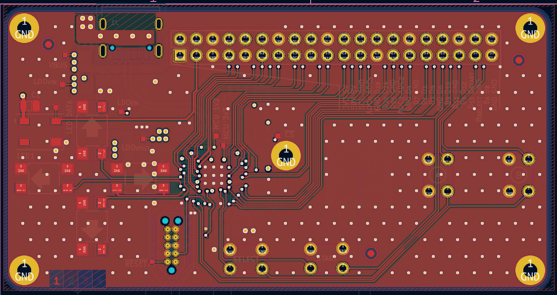
You can probably notice that there are 4 of the 8 buttons, the D-pad buttons, that are surface mounted, but this would have required assembly on two sides of the board. The design is supposed to have a complimentary number of through-hole targets, so that students could get some practice with both styles of assembly.
The board nets a cost in quantities of 500, of about $3/board. This was a bit on the high side, given that potentially thousands of students will end up assembling it.
 There are some design quirks with this, partially because I was trying to be more creative with trace with control, but the placement of the vias is uneven and messy, and I knew during the design work that it could be touched up.
 The sizing of the decoupling capacitors (0603 imp.) is large given the intended ESR and form factor recommended in the RP2040 hardware design checklist, but even these are probably too small for people who have not soldered with a stencil and hotplate before.
Among other things is the layout and fanning out of the traces from the MCU. Not my best work, so doing this again was probably for the best.
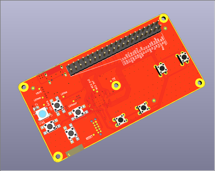 Overall, the board looked nice, but was kind of rushed and not really what I wanted. Walking away from it, I knew the debug header did not need to be there, it was not easily assembled by complete novices, the components could be cheaper, the placement could be better, and the physical size should be smaller (lower cost, easier to use on the miniware hotplates).
Discussions
Become a Hackaday.io Member
Create an account to leave a comment. Already have an account? Log In.