Check. It. Out!
The first board has been assembled! I placed the buttons on the opposite side (Intentional, and a great demonstration of one of the assembly of the board; Placing the through-hole components on either side has zero effect on functionality. Students always screw that one up.)
I did however... forget to purchase the USB connectors, the right sized USB termination resistors, and... the fixed LDO regulator. I guess that now explains why the order was $400 cheaper in reality.
The "Correct" (D-pad is on the left) orientation looks like this:
Which is the board my friend put together with me. You can probably spot the exposed via's. That was, I suppose not really my fault, but a problem with the PCB order. The JLC plugin I was using seems to have overwritten my soldermask expansion setting, resulting in the unfortunate complete exposure of every single via.
Assembling the board myself, I was able to get everything on there around the MCU without serious shorts, but it does concern me for the broader student audience. Functionally the board will be fine.
Stay tuned for when I fix all my mistakes, for the next iteration of the boards.
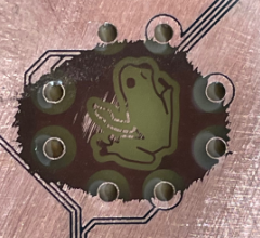
Easter egg:

 micl
micl
Discussions
Become a Hackaday.io Member
Create an account to leave a comment. Already have an account? Log In.