Update 20170404: superseded by New DRAM array
I have received "some capacitors" as well as "some diodes". The surface-mount LL4148 were meant for program wiring but the little gotcha with the DRAM made them even more important for temporary data storage.
I have to redesign the capacitor arrays and these diodes are pretty critical because they consume a bit more of PCB real-estate. Oh and they can be very tricky to solder.
I have chosen to save a bit of surface with a little naughty trick : solder them back-to-back, sharing a PCB pad. This saves maybe 2mm in one dimension and should not affect reliability. This means I have to redraw a new part in Eagle...
Let's have a look at the specs of the chosen packaging (I have actually "chosen" the lowest bidder, to be honest, not minding the increased soldering efforts).
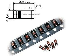
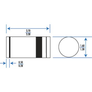
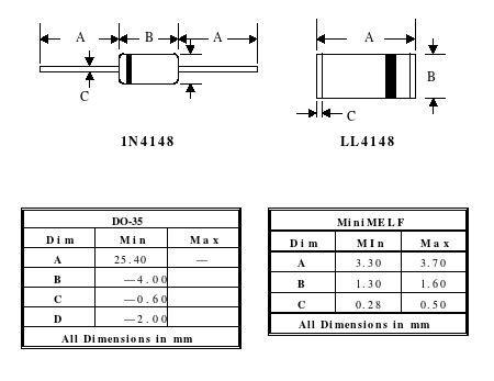
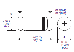
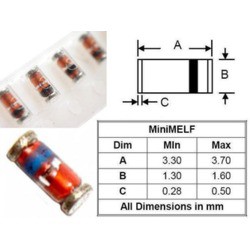
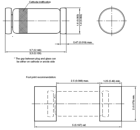
I'm trying to determine the agreed upon miniMELF/DO35/SOD80/LL34 (pick your favorite) packaging dimensions. Most people use the 3.3-3.7mm length...
The last screenshot shows the recommended footprint. My idea is to merge one pad with the pad of the neighbour diode. Normally, there would be at least 2×5mm but the merge saves 1.25mm, giving a length of 8.75mm. This is still quite long, longer than the capacitor's diameter. Routing will be fun.
Another approach would be vertical soldering. Density certainly increases, as well as other kinds of headaches. I could make a tool to keep the diodes upright during soldering but the next step (connecting all the leads in the air) is less deterministic...
Through-hole parts create their own kinds of problems. When space is constrained, the hole uses space on both PCB layers, but this area might be precious or critical on one side, for routing stakes.
My current idea is to create a "part" in EAGLE with the capacitor and the two diodes, and rotate every other by 180° to fit everything in the 6mm grid... Hoping it will fit...
I have DRAM capacitors (25V 100µF) both in 5×11 and 6×7mm formats. Both seem happy with 0.1" spaced through holes. That's a good starting point for the new composite part.
So I created this symbol:

The footprint is constrained by the size of the capacitor :
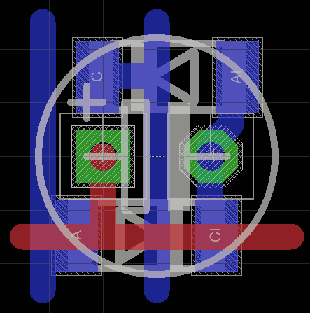
I have chosen a grid of 6.35mm (1/4") which is a tiny bit larger than the 6mm of the previous attempt. It shouldn't be too hard to solder manually. I have given up on trying to solder the diodes back to back, the above pattern is easily integrated as an array:

Just put the cells close to each other, snapping on the grid, and voilà.
I have tried a 16×32 array, which is a bit larger than 10×20cm (without the mux16 and connectors). The total capacity with 16+1 slices is 512 words, or 8Ki bits, or one kilobyte. I might postpone the soldering of all the parts... Because of the "screen", initially I need maybe 64 words at first (4 columns, 1K capacitors).
In theory, I can drive all the vertical wires of all the boards with a single 64-mux, the total relay count is therefore: 64+ (16×17)=336. Add to this the refresh logic, the data and address MUXes, the sense and buffers, and the DRAM system uses about 500 relays as expected...
Some questions remain :
- are there any more gotchas I have to care about ?
- I have "solved" the partition of the MUX16, is there a solution for MUX32 ?
- how long will the capacitors keep enough charge with the couple of diodes ? I suspect that a higher leakage will affect the refresh cycles. 512 words at 10 refresh per second (optimistic average) means that the whole array is refreshed every minute...
This can be answered with a magic circuit called a prototype ;-)
 Yann Guidon / YGDES
Discussions
Become a Hackaday.io Member
Create an account to leave a comment. Already have an account? Log In.
So the DRAM uses electrolytic capacitors?
Are you sure? yes | no
My circuit uses electrolytic capacitors.
DRAM chips as used in your computer use a different capacitance (gate-source capacitance of ultratiny MOSFETs) which don't need the diodes. But you can't use this at the macro level, hence my design.
Are you sure? yes | no
I found the logs for this entire project fascinating, but this particular topic stood out to me. The type of capacitance isn't the reason for not needing diodes; capacitance is capacitance. If you were willing to use MOS transistors as pass gates, you can also get away with using single-transistor switches too.
The reason for using the diodes is because you are routing a single voltage source to a single voltage sink through the matrix as a whole. You need two switching elements (one for horizontal and one for vertical directions). The reason why DRAM chips use the single transistor switches is because they transfer an entire **row** of voltages to a sink all at once; thus only one switch is needed because only the vertical direction is considered. For instance, if you have a 16-by-16 matrix of storage capacitors on a DRAM chip, you'll have a row-select signal which opens the pass-through transistors across the entire row. This means you must also have *16* sense amplifiers and drivers to write-back the data, since reading the data from DRAM (as with core memory) is a destructive operation. (This explains both what "precharge" is in DRAM timing diagrams, and why simply reading a location in DRAM is sufficient to refresh the entire row in which that location is stored, BTW.)
Hoping this provides some explanation for why one design uses dual-diode switches while the other, commercial, DRAM chips use single pass-through transistors.
Are you sure? yes | no
Samuel : You're right, but here I can't use so many pass elements, the cost, power and space would be unbearable :-D
They have it soooo easy with integrated circuits...
Are you sure? yes | no
I built a voltage multiplier out of free standing caps and diodes. :)
In your case, may be tag down some toothpicks as rails for lining up those diodes as they can row around.
Are you sure? yes | no
Very pretty ! are you prototyping a USB killer ? :-D
Are you sure? yes | no
It was a 20X voltage multiplier for about 20kV. I played with lifter and a few things. I blew up something in there. It doesn't lend itself for repairs unfortunately.
Are you sure? yes | no
Repairs are a pretty critical aspect, you can get away with 10 stages, but I'll have 8K and the probability that something goes wrong is close to certitude. If I can't spot failures and repair them, the whole endeavour will fail... I'm routing right now :-)
Are you sure? yes | no