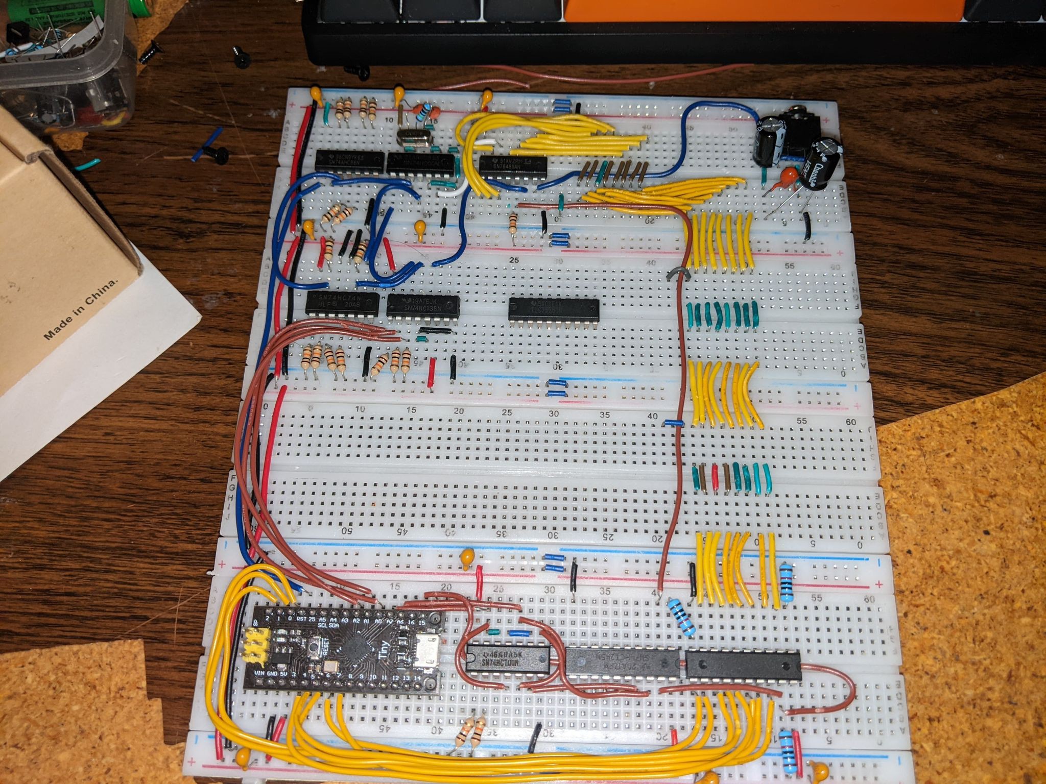
So for starts I am building a rough bread board prototype, which i can control with a easy to program attiny88 dev board ( I use a cheep USB programmer as the usb ports on these are practically worthless.) I can run a simple test program at the moment that sets the registers in the PSG (using the control logic on the bottom board (all HCT). Next is to hook up the FIFO module, and get it to do write through:
- Write through will pass along the current data to the PSG / DAC immediately following the rising edge of /WRITE signal from the control logic.
- The buffer will hold the data only if the PSG or DAC are not ready to receive the data (which at normal speeds wont likely be more than a clock cycle.)
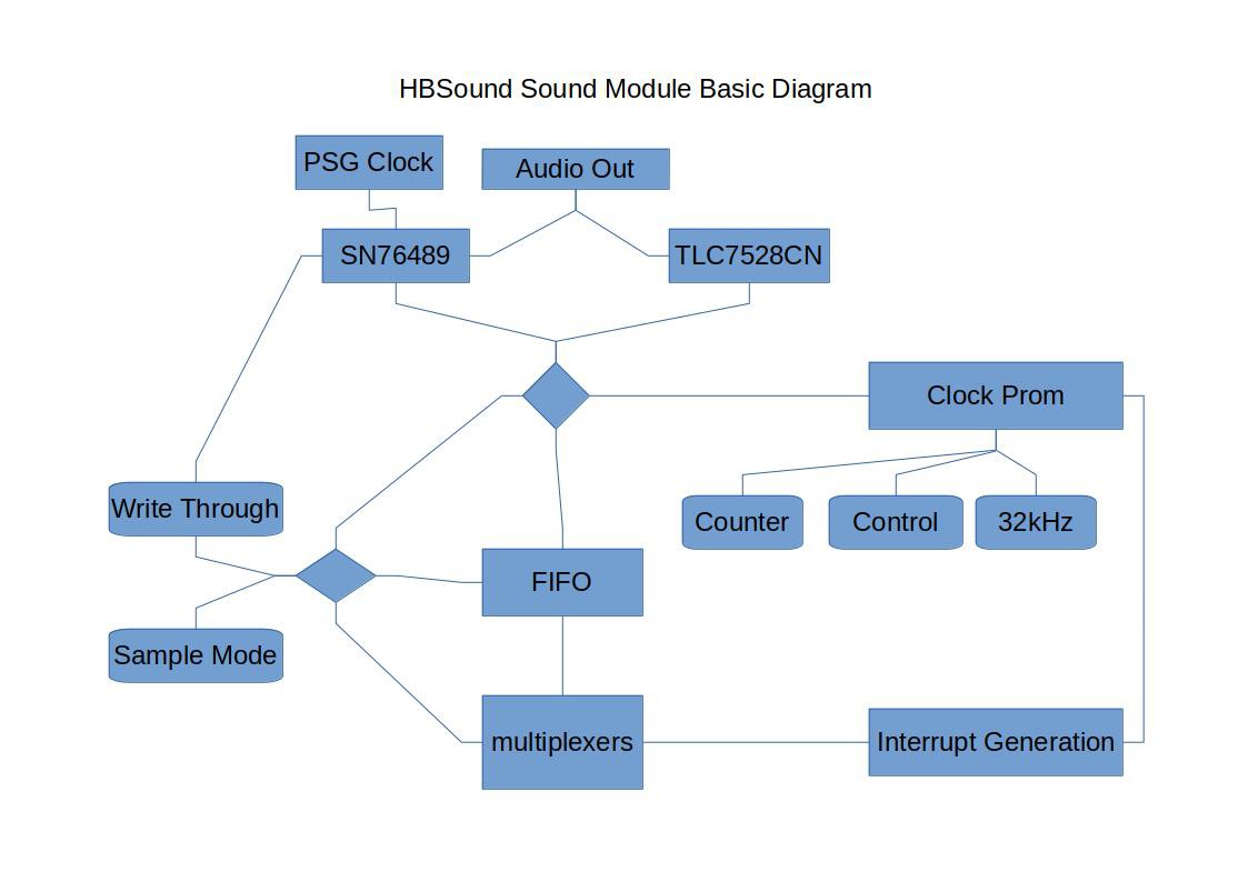
After that is working, I will start work on a design to implement an adjustable clock, with interrupt generation as an option that can be used to set a sample rate based on a maximum of 32 kHz. The basic diagram for the card is as follows:

The design is still fluid, but I am hoping once I get the kinks worked out of write through I should be able to proceed on to getting the TCM (Timer / Clock Module) finished.
 Dave Collins
Discussions
Become a Hackaday.io Member
Create an account to leave a comment. Already have an account? Log In.