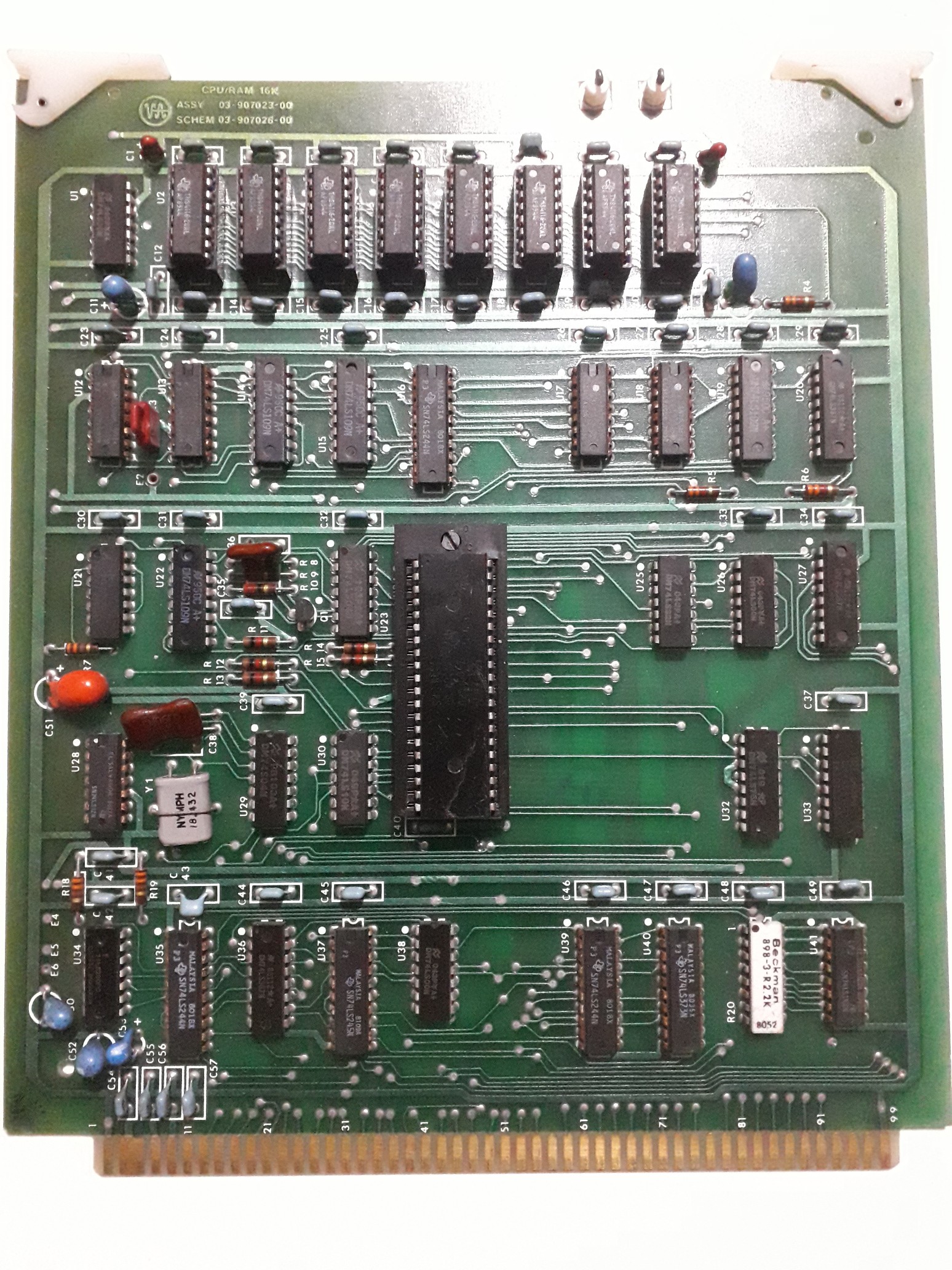
The CPU board is now almost fully probed out. The schematic is not the tidiest, but all the chips now exist, though a few pins still need checking out. A lot of the signals I can work out the function of from their connections to pins or other identifiable signals, but there are a few I'm still unsure about. There may also be some mistakes, I'll have to recheck everything once it's complete.
If I'm reading the /RAS circuit correctly, the onboard 16K of RAM sits in the uppermost 16K of memory from &C000 - &FFFF. Unless I'm missing something, I can't see any bank select logic on the board, so the RAM card must handle that itself. I also don't see anything to stop the address/data lines being active on the bus during access to local RAM, so I assume the RAM card must handle mapping itself into a suitable place in the memory map so it doesn't respond. I'd assume U37 needs to turn off though, so floating inputs on the BD[0..7] lines aren't making it try and drive D[0..7]. Maybe the /DBUSEn logic handles that.

Discussions
Become a Hackaday.io Member
Create an account to leave a comment. Already have an account? Log In.