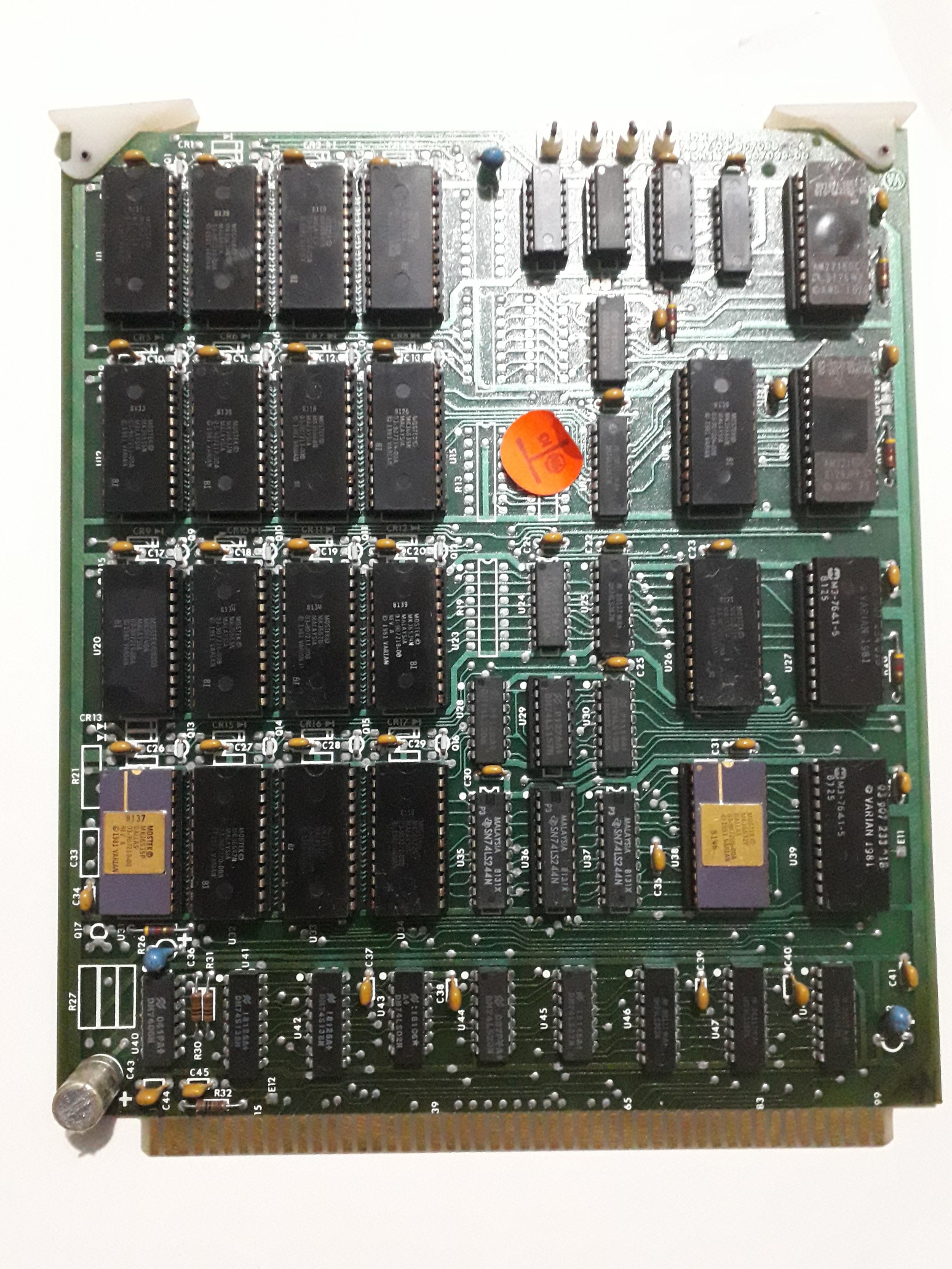
The ROM PCB seems to be split into three primary sections:
The left hand side consists of 16 8KB mask programmed ROMs, addressed via two 3-to-8 decoders. These are the system's paged ROMS.
The mid-section consists of 3 8KB mask programmed ROMs, permanently mapped into the address space. These are presumably the core OS.
The right hand side consists of 2 512B mask programmed ROMs serving as some kind of additional address decoding logic, and 2 2KB EPROMs. I have yet to work out where these two EPROMs sit in the address space visible to the CPU.
The memory map, thus far, appears to be as follows:
| Start | End | Contents |
| 0000 | 1FFF | Fixed ROM U18 |
| 2000 | 3FFF | Fixed ROM U26 |
| 4000 | 5FFF | Fixed ROM U38 |
| 6000 | 7FFF | undefined |
| 8000 | 9FFF | Paged ROMs |
| A000 | BFFF | undefined |
| C000 | FFFF | CPU local RAM |
I haven't looked at the RAM card yet, but I assume there will be a 3-to-8 decoder mapping that 64KB into 8KB pages in one of the two undefined spaces.
The paging latch on the ROM card sits at IO address 0110xxxxb. Rather than latching the data bus, it latches the lower four bits of the address.
Discussions
Become a Hackaday.io Member
Create an account to leave a comment. Already have an account? Log In.