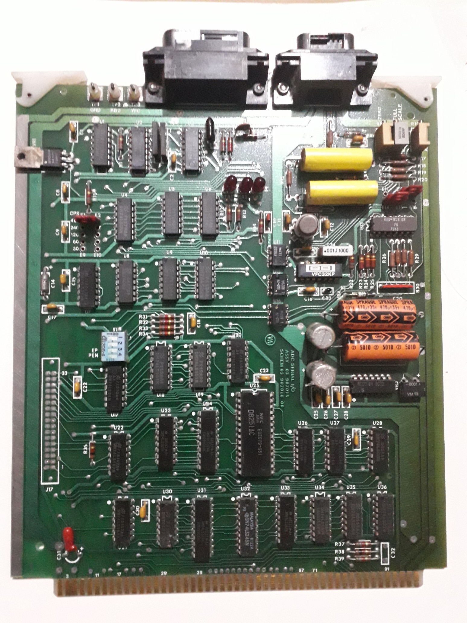
This board turned out to be far more complex than expected. There are three connectors on the board - a large 24 pin connector wired to the 8251 PCI, a 14 pin connector wired partly into the digital side, and partly into the analogue side, and an unpopulated 34 pin header.
Based on the probing so far, I suspect the 14 pin connector is the link to the chromatograph machines, and it has some bit-banged protocol driven directly by the CPU when needed. I haven't looked into the analogue circuit yet, but I assume it's an ADC and associated reference voltages. A couple of optoisolators link from the digital side.
The 34 pin header I am guessing is for attaching a precision ADC. It consists of a read-only 14-bit parallel interface, read as an upper 6 bit number with a seventh bit fetched from elsewhere, and a lower 8-bit number, mapped into different addresses. The address used to write to the analogue port is the same as the address used to read from one of the header addresses, which, combined with the 14-bit data length, is what makes me think its ADC related. None of the four boards I have have this populated, so it was clearly an optional extra.
The serial port is a centronics-style socket so I will need to make an adaptor or wire another socket directly to the board to make it talk to anything else.
The schematic is unfinished and needs rearranging because it turns out chips are scattered all over the board with no regard for which other chips they are connected to. The logic surrounding what are supposed to be the interrupt and acknowledge signals makes no sense in this context, so I think these pins have been repurposed. In particular, Int7 and IntAck7 are wired into the chip selects, and I assume are hardwired on the backplane to give each of the four serial slots a unique address. Having a backplane to look at would make this much easier.

Discussions
Become a Hackaday.io Member
Create an account to leave a comment. Already have an account? Log In.