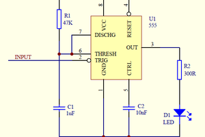
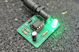
555 timer is one of the most advanced and most popular IC of it’s time. This IC has a lot of configurations and circuit arrangements. We can design some small sections of a circuit using this IC without using any microcontroller. This IC has some applications in generating square wave up to 500khz with an adjustable duty cycle, generating precise time delays under monostable mode, bistable mode to make a two-latch switch configuration and Schmitt trigger. Other some applications with this IC are single button latch, 50% duty cycle free running oscillator, PPM, PWM, Ramp generator and touch switch. But here we are only discussing the astable operation of this IC.
Astable mode is auto triggered configuration of this IC which is used to generate a specific duty, frequency square wave. But before discussing more about the configurations let’s have a look on internal circuit and the pin diagram. Which will help to clear the 555-operation theory and working later on.

Then we will made a PCB of the project and order it from PCBWAY. PCBWAY provides the prototyping service in very low prices. Get your PCB boards just in $5 for 10 Pcs of 2 layer boards. It is fully custom service, choose your PCB specs according to the needs and get Quote within 5 minutes.
Internal circuit:
This IC has 3 resistor of 5K which together makes a voltage divider section. These 5K resistors divides the input voltage into 3 parts, first is VCC, then 2/3VCC and VCC/3. Two comparators are attached to those 5k resistor terminals AT 2/3VCC and VCC/3. The inverting terminal of comparator one is connected to 2/3VCC and non-inverting to the threshold pin. The non-inverting terminal of comparator two is connected with VCC/3 and inverting terminal to the trigger pin.
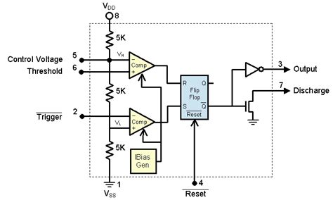
Then you will find a SR latch, and the output of comparators is the input of this latch. There is a PNP and NPN transistor configuration also one for the reset of this latch and other one is connected to the Discharge pin of the IC. The special thing about this IC is that it can generate very accurate time delays.
Pin diagram:
There are 8 pin in the DIP package of 555. It is made by Texas and nowadays manufactured in ST labs. These 8 pin of the IC are arranged as given in the Image.
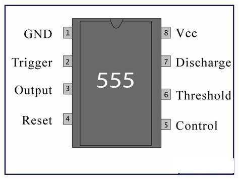
For more package info download the original datasheet from here. Some more features are:
Output Can Source or Sink 200 mA
Output and Supply TTL Compatible
Direct Replacement for SE555/NE555
Normally On and Normally Off Output
Temperature Stability Better than 0.005% per °C
Astable configuration:

In the astable mode of this IC, the following circuit diagram is used. Capacitor is connected to 2,6 pin. Reset pin(4) is connected to VCC(8). Trigger(2) to Threshold(6) to make a loop or auto trigging circuit. Control voltage(5) is connected to ground with a bypass capacitor to avoid any noise. One resistor R1 is connected between pin 6 to 7 ( Threshold to discharge) and R2 is between 7 and 8(discharge and VCC). This configuration is only used for a stable mode to generate a specific frequency with fixed duty cycle. Let’s know what is happening inside to calculate duty cycle and frequency values.
Working of Astable mode:
When initially power is turned ON, Trigger Pin voltage is below Vcc/3, that makes the lower comparator output HIGH and SETS the flip flop and output of the 555 chip is HIGH.
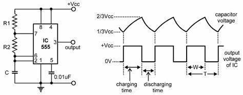
This makes the transistor Q1 OFF, because Qbar, Q’=0 is directly applied to base of transistor. As the transistor is OFF, capacitor C1 starts charging and when it gets charged to a voltage above than Vcc/3, then Lower comparator output becomes LOW (Upper comparator is also at LOW) and Flip flop output remains the same as previous (555 output remains HIGH).
⦁ Now when capacitor charging gets to voltage above than 2/3Vcc, then the voltage of non-inverting end (Threshold PIN 6) becomes higher than the inverting end of the comparator. This makes Upper comparator output HIGH and RESETs the Flip flop, output of 555 chip becomes...
Read more » Lithium ION
 Jan Waclawek
 Melvin van Kalsbeek
 Hulk
Hulk