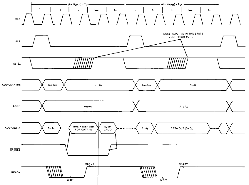
Ah HAH! The 8288 doesn't *need* the "READY" signal... it bases its actions on the /S2:0 signals, sent by the CPU.
(This may sound obvious to you, but I spent *numerous* hours tracking down signals in schematics before coming to that conclusion.)
If I understand correctly... this may be a *tremendous* advantage...

Again, the CPU is responsible for responding to the READY signal input. And it does-so by basically delaying everything until READY is true... and it goes about delaying the *bus* by keeping /S2:0 in their current state.
This, again with the SRAM example, is the equivalent of keeping the /RD or /WR signal active for an extended amount of time. That's no problem.
So, let's say it takes three instructions to read a READY signal, and jump back to the ready-test if it's not ready... And, say that's running at the bus-clock... so, technically, it would take three bus-clocks just to process the READY signal. That's *in no way* within the specs of the 8088, which can handle it within a single bus-clock. BUT, it shouldn't matter, right?
So, if the device is ready, immediately, we'll waste 3 bus-cycles reading that in, and breaking from the loop... The effect, then, is just that the CPU itself added 3 wait-states of its own. (Which isn't spec'd anywhere, but, now, seems like it should work).
If the device is *not* ready, immediately, then we'll only be able to test it once every three bus-clocks... Oh well.
So... I think the ready thing is resolved.
(Note that all this relies on the fact that I'm *not* using an 8087 FPU, nor the DMA controller, or other things that might try to take over the bus).
----------------
Here's a more programmatic view of the timing-diagrams...
Modified a bit for an AVR... but not yet including my READY-processing with a 1:1 AVR:Bus clock-ratio.
## IDLE ##
   A19:16
   A15:8
   A7:0
   S2:0 //Begin transaction
## T1 ##
    (8288: ALE Low, immediately before T2)
## T2 ##
    (8288: /WR low (WRITE))
    *right before CLK^*
     A7:0 -> Input (READ) / D7:0 (WRITE)
   (CLK ^)
    A19:16 -> S6:3
     (8288: /RD low (READ))
## T3/Tw ##
    --SAMPLE READY/!WAIT
     (READ: "Bus Reserved for data in")
    IF READY (FALSE, for this example)
      S2:0 = IDLE
      (CLK ^)
      (8288: /WR high (WRITE))
    ELSE
      Repeat T3, call it Tw
## T4 ##
    --SAMPLE (READ)
    (8288: /RD high (READ))
    D7:0 -> float (WRITE) (PROBABLY only need for bus-masters, DMA, etc.)
   (CLK ^)
## IDLE ##
So, now, I think the only thing remaining to be figured out is how to handle T2 which has two instructions: Modifying AD7:0, and outputting S6:3.
(Oh, and I've been ignoring the /QS bits, I think those are only required when using an FPU. The same might be true for S6:3...?)
-------
Hahahaha! Ridiculous!
The "bus masters" such as the DMA controller, interface... *with the bus*... I dunno why I didn't think of looking at them, instead of the 8088/8288.
And, yahknow, I don't think they implement things like /S6:3, etc.
 Eric Hertz
Discussions
Become a Hackaday.io Member
Create an account to leave a comment. Already have an account? Log In.