-
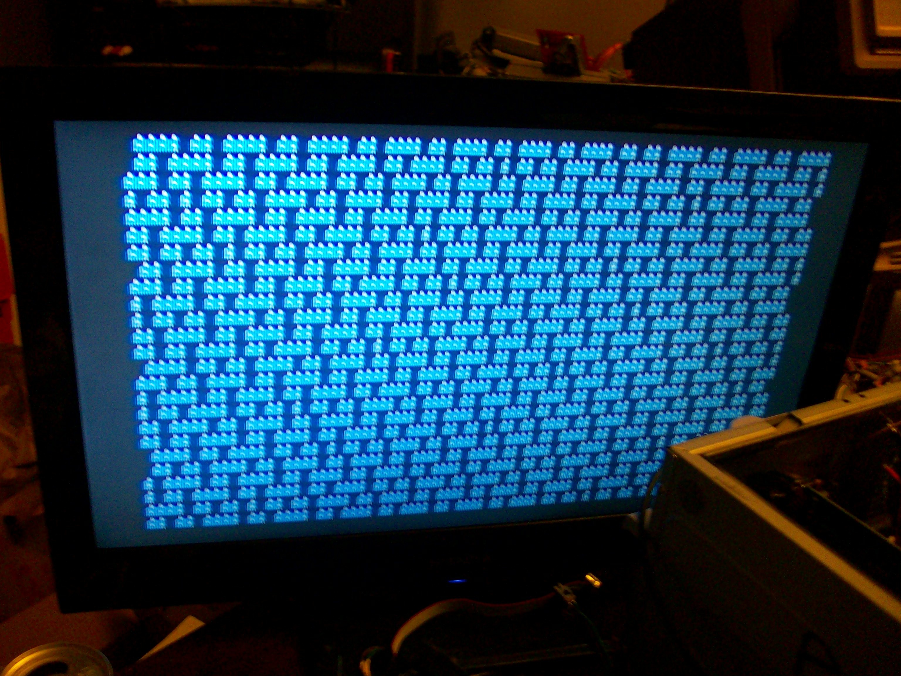
WE HAVE CGA!
02/04/2017 at 18:03 • 11 commentsUpdate: Random thoughts on potential explanations to be explored. (at the bottom).
-----------------
WE HAVE CGA! -ish...
So, technically, it's supposed to be All A's... but what canya do...? Looks kinda cool, a bit like a video game town.Or a wall of bricks, maybe legos... maybe I'll try red on gray.
There seems to be a somewhat regular pattern, maybe having to do with my bus-timing not being 100%. (almost speaks to me of 'beating' in the physics sense, which would make more sense if my AVR clock and the Bus clock weren't synchronized). Though, the DRAM verifies are still giving only one error in 640KB... So, maybe the ISA CGA card has slightly different bus-timing requirements.
Over all, this is pretty exciting... My old-school Atmega8515 8-bit AVR sitting in an 8088 CPU socket, driving an ISA CGA card...
----------
Haha! All I changed was the background/foreground color attributes...
This looks real cool.
Herein we've got numerous factors at play...
My CGA card is known for being a bit flakey... (see previous logs) Combine that with an LCD, rather than a CRT, and there's some other interesting effects...
Now we've added flakey bus-interface...
But how can this pattern possibly be explained? What I programmed, again, is a full screen of nothing but the letter A in red on a background of white.
Perty durn cool, though.
--------
Hah, fewer factors at-play than I thought...
Though, the LCD definitely seems to be syncing differently on different colors, whereas the CRT has pretty sharp vertical edges.
---------------------------------------
UPDATE: Thoughts On Why:
Frankly, I'm a bit excited by the weirdness of this. Realistically, its coming up with much more interesting visuals than I would. (See the next log)
I copied most of my CGA-initialization from the PC/XT BIOS Assembly-Listing, (converting it to C). (I'll throw that file up in the files section). But, there are definitely some x86 instructions I don't understand, and parsing it was a bit of a mind-bender for me, some of it I just threw up my arms and made assumptions about what the goal was. So it's plausible I missed some initialization-stuff. Also I skipped over some parts, like the bit that clears the memory. (What a weird idea that there's a machine-instruction that can load a value to 16384 memory locations!).
Aside from that, it seems some parts of the initialization appears to be interspersed in numerous locations across dozens of pages of otherwise unrelated assembly. So, it's even more likely I've missed something. Also, I didn't have the patience to stare at even more assembly to implement the remaining INT10 (video-I/O) functions... After I finally got initialization coded-up, I just started writing data to the VRAM.
Also, I vaguely recall something about a portion of the memory being used for the character-set above 0x7f, so I should look into that.
There's also some info 'round the web regarding the card's registers. I didn't look hard, but get the impression the majority of those aren't low-level enough to explain the *very initial* initialization-process... those I found seem to presume the card's already initialized (and you wish to reconfigure it). Though, I'm willing to bet that low-level info is out there, and probably in greater-depth than ever, what with the decades, and the demoscene.
Also interesting to note: I broke the DRAM write/verify routine up a little bit: instead of writing all 640K then reading it all back (which took about 4 seconds), it now handles that in 256 chunks, that way I can do some "realtime" stuff in the meantime... And... Now the DRAM shows no verification-failures! So, at least as far as that goes, interfacing with the bus is pretty reliable. Earlier verification-failures must've [still] been refresh-related.Though, as I found out a log or two ago, different types of memories (and I/O devices) respond differently to the "typical" memory-bus: DRAMs apparently latch their writes on the falling-edge of /WE (?!), whereas SRAMs usually latch on the rising-edge. So, the 8088's strict bus timings may very well be designed to handle a variety of different cases that my timing doesn't quite match-up with.
It's also quite plausible the CGA card is flakey... The images it displays are definitely weird (illegible in most cases, even in DOS), and its ... OH MAN I bet I got it (I'll come back to that). The card was quite corroded, requiring quite a bit of cleanup/reflow. It's entirely plausible I have some DRAM address/data lines shorted or traces that've been mostly-degraded.
"OH MAN, I bet I got it": It "looks a bit like beating," right...? And In part of the effort getting the card cleaned-up and functioning I installed a separate crystal oscillator on-board, separate from the ISA's clock. Seems odd to me there was a place for a separate crystal, if it requires the timing to match the system-bus, but that'd sure explain the "beating."
Also, now that I think about it, there's a specific register to read-back, indicating that it's OK to write to the VRAM, the BIOS pays attention to that in some of its routines (which were too many and too long for me to translate to C). I *thought* that was only to prevent the "snow" effect, which occurs when you write a memory location at the same time the raster-drawing tries to read it. But maybe there's more to it than that. Hmmmm....
------------
As far as write/verify to the VRAM, I hadn't tried that before posting this log. I've since added a "counter" displayed in the upper-left corner of the screen, indicating the attribute-settings used... (It was *hard* finding attributes that would display clearly! But that was a problem with DOS and my BIOS-Extension, as well)... But, in implementing that, it definitely had some issue displaying the number. First I tried writing each character 10 times, but it'd overwrite some with spaces (interestingly, almost always spaces.... maybe 0xff from pull-resistors? hmmm), and sometimes different attributes. So, then, for those important characters I did write/verify loops until verified correctly. Not quite read-back of the whole shebang, but a test (and no indication of how many times it takes to get right...)
And... no... My bright-idea regarding "beating" doesn't make as much sense... as I thought... Because it works with DOS (despite being illegible).
-
Write-Read DRAM works-ish! + Manual-Refresh
02/04/2017 at 01:12 • 6 commentsLoading somewhat-random patterns into the entire 640KB of DRAM, then reading it back... It takes about 4 seconds for a full write/read/verify.
DEFINITELY consider refresh.... Failures increase dramatically as printing a failure takes a bit of time, and that adds to the delay in the refresh of the later bytes, compounding the problem.
So, I've looked into the schematics as best my brain can absorb, and I get the impression that the DRAMs are addressed as such: A15:8 are used to address columns, while A7:0 are used to address rows. When opening a row, as I understand, the entire row gets refreshed (read or write). The higher address-bits (A19:16) select the DRAM chip (and/or are used to select higher row/column addresses... this is where my brain gets lost).
So, as a quick test, I figured to do the following:
Write *all* data locations with data that can't be mistaken from byte-to-byte... (some XOR combination of the address and some other stuff)...
Byte0: 0x00000
Byte1: 0x00100
Byte2: 0x00200
Byte3: 0x00300
...
Byte 255: 0x0ff00
...
Once you reach the maximum DRAM address (0xA0000), start again:
0x00001, 0x00101, 0x00201, and so-on.
------
So, now, with every (sequential) memory access, a row is refreshed. So, whereas before an entire refresh was taking about 4 seconds, now it takes 4/256 = 1/32nd of a second to perform a full refresh.
.
Can't say I came up with the idea... I read vaguely about it on some demoscene page, I think. (I gotta say, I never had much respect for the demoscene until I started this project). As well as some looking into the BIOS code, which, as I understand, basically sets up the DMA controller to do essentially the same. Looking at the schematics (and not really understanding the DMA controller) I think it's slightly more sophisticated than this. There's a bit of circuitry that allows strobing *all* the /RAS pins on *all* the DRAM chips simultaneously. But that circuitry doesn't appear to be accessible any other way than through the DMA controller.
And, I'm sure my method could be improved with further understanding of the circuit. E.G. the /RAS signals go to all the chips within a bank, /Chip-selects are scattered-about, as well. And there's the higher address-bits which go to higher row/col(?) addresses. And, I haven't looked into it very thoroughly. So, e.g., if there's some combination where multiple chips are selected, but their output-enables are demultiplexed, all those chips would be refreshed simultaneously. (I know that SDRAM DIMMs wire things up in this way, it's a scheme for adding more addressable-space, without using explicit address bits. But it also serves the purpose of running the same instruction on those chips, even if that instruction serves no purpose (e.g. READing from a bank of chips while all but one have their output-enables disabled... the read-access occurs, but it's hidden from the user. But it also refreshes all the chips).
--------
As it stands, I'm now getting only one verify-failure through every write/read/verify loop of all 640KB!
-------
The problem, from before, apparently was due to a misunderstanding of the timing... I'd *intended* on activating the /S2:0 signals during the end of "T4", but it turns out it's activating at the beginning of "T1". So I had a nop where it wasn't necessary. I still need to look into that more thoroughly, but earlier tests (before I implemented refresh) were giving only 3 verify-errors out of 640K (but those were read immediately after written)... and I tried all three clock-delay options with no noticeable change. So maybe the clock-alignment isn't nearly as picky as I'd feared. Or, maybe that explains why I'm still getting a failure...
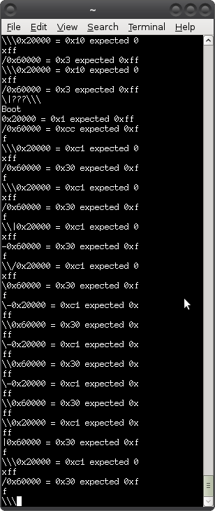
Here's the output from the tests: ("COUNT" is a bit misleading, it's <<=1)
Boot
0x20000 = 0xf0 expected 0xfe
0x60000 = 0xde expected 0xfe
0x1ef45 = 0x44 expected 0x54

### COUNT = 2 ###
0x1ef45 = 0x47 expected 0x57

### COUNT = 4 ###
0x1ef45 = 0x41 expected 0x51

### COUNT = 8 ###
0x1ef45 = 0x4d expected 0x5d

### COUNT = 16 ###

### COUNT = 32 ###
0x1ef45 = 0x65 expected 0x75

### COUNT = 64 ###
0x1ef45 = 0x5 expected 0x15

### COUNT = 128 ###
0x1ef45 = 0xc5 expected 0xd5

### COUNT = 0 ###
0x1ef45 = 0x45 expected 0x55
-
But no write...
02/03/2017 at 19:50 • 1 commentUPDATE 3: DRAM CAS/RAS via delay-line... interesting. At the bottom.
UPDATE 2: Yep... DRAM latches on falling-edge. At the bottom.
UPDATE: Surprising result added at the bottom
-----------------
Seemed like a simple step from read to write... but so far it appears to be writing the low address byte to the DRAM, rather than the data.
This is kinda confusing... Or at least, surprising.
I'm not familiar with DRAM (SDRAM, SRAM, a bit... but not DRAM).
So maybe there's something in there...
If this were SRAM: As I recall: When the /WE pin is active, it'll write to the selected address. So, if the address stays constant (which it does, since it's latched), the data could change numerous times before the /WE pin is deactivated, and whatever was on the data-port last (assuming a long enough setup/hold time) would be stored in the memory.
So, e.g., it would be doable to wire the SRAM's data pins to the shared/multiplexed Data/Address port, to load the address to that port, to latch the address (in an external latch), then enable /WE (with the address on the shared address/data port!), then (after /WE) change the low address/data port to the data to be written (address has been latched, remember?)... let it "stabilize" there for a bit, then disable the /WE pin. Technically, the memory-location would store the low-address-byte for a brief time, but then it'd be overwritten with the data... so, as far as anyone would see, it'd look like it worked as-expected, were the /WE pin *only* active when the data was on the port.
This is, entirely, as I recall... I could be mistaken. Regardless, certainly whatever's loaded is that which was valid when the /WE pin toggled from active to inactive. Right?
----------
Frankly, it shouldn't matter whether DRAM works differently, as long as it latches the data when /WE deactivates. And, frankly, it shouldn't be any other way... because... the bus could be held-up by wait-states (which apparently has less to do with the actual time it takes to access slow memories than it has to do with waiting for other things holding up the bus, e.g. DMA... per my understanding of the schematic).
Which Means...
...No. Because if the bus is held-up, the READY signal indirectly deactivates the 8288's CEN input, which disables the /WRITE signal. (and, oddly, causes the timing-diagram to be distorted, because /WRITE is shown active during T3, but with CEN disabled (which is supposed to happen before T2), it would become active *after* CEN is reenabled.
OK... So, it's plausible... Though completely beyond my intuition, that data is stored upon /WE's activation. edge-triggered on the opposite edge I'd've expected...(?!)
Let's pretend that's the case for a second...
Then timing needs to be much more precise than for read-operations.
And uC-inserted "artificial wait-states" won't work... at least with regard to being able to use that time to help set up data. (They do, however, still appear to affect the deactivation of the 8288's /WRITE pin, as 'scoped).
That timing-precision...? Because the address has to be latched, which happens near the end of T1 (and requires a hold-time thereafter), then the data has to be available by the beginning of T3... Only slightly longer than one clock-cycle. Which should be *plenty* of space to work within, but also quite a bit more timing-sensitive than the read-operation... So maybe those inverter-clock-delays and cycle-counting with NOPs are more important than read-back led me to believe.
This, too, might suggest that even if I get one device working smoothly with whatever wonky timing-scheme I might come up with, doesn't necessarily mean it'll work with another... So maybe it's a good thing I spent so much effort looking into those timings early-on.
Got some 'sperimentin' to do. First things first: Clock-Delay jumpering. Then NOPs that can likely be removed (carefully! Keeping clock-delays and setup/hold times in mind!). And, from there...? I read somewhere the AVR's internal clock doesn't necessarily align with the external clock input... so might be necessary to characterize that, a bit.
Kinda funny, I thought write would be less timing-sensitive than read...
-------------
Another possibility supporting the awkwardness of /WE's apparently latching on its falling-edge could be an intermediate data-latch that I'm not seeing. I glimpsed through the schematic and don't see it, but who knows. The DRAM circuitry's a bit complex, what with row/column strobing, etc. (Before I started this project, it hadn't occurred to me they would implement that scheme with simple logic gates, making it *look* like a regularly/linearly-addressed memory. Interesting ponderance to throw at #sdramThingZero - 133MS/s 32-bit Logic Analyzer)
Interesting observation:
The DRAM (even this really old stuff) apparently retains its value for *quite some time*. I turned off the computer for several seconds and it still read back most of the data written.
------------------
UPDATE: Huh, removing this NOP gives darn-near 100% write/read verification...
I'm pretty certain that nop needs to be there. And changing the AVR's clock-delay doesn't seem to have an effect. Definitely some thinking to do.
![]()
![]()
brainjuice running out... interesting pattern, though.
--------
SRAM:
![]()
Latches on rising-edge...
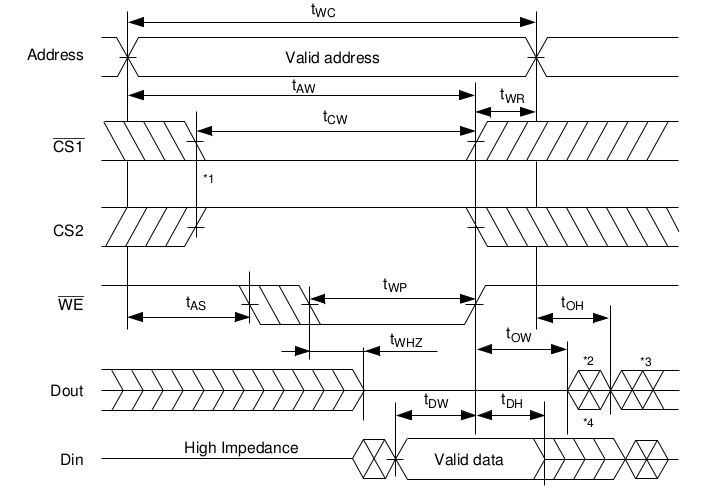
DRAM:
![]()
Latches on falling-edge.
------------
Am thinkink the reason the 8088 bus-timings are *so strict* is because it's meant to work with various different devices. So, for instance, can probably handle both SRAM and DRAM. (And here I thought these interfaces were pretty much standard... why call it /WE at all? Why not WE, or better-yet WCLK... wait, isn't there a "C" in the 8288's write-signals... hmmm... /MWTC "Memory-Write COMMAND" heh.)
--------------
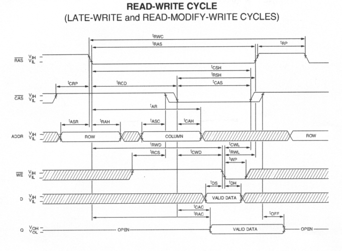
Check this guy out:
![]()
So basically the Row-Address is strobed, then a delay-line(?) signals to load the column-address, then creates the Column-Address strobe.
And I've yet to find anywhere where an onboard memory-device requests wait-states... (only the ISA cards and DMA, so far). Interesting that all these subsystems are running at, basically, the same speed. DRAM I'd've thought would be slower, at the time. Not only slower, but also slowed by the fact of random RAS/CAS accesses. And, yet, if I understand this correctly, the DRAM actually responds to a full-speed 8088 bus transaction with no wait-states. Similarly, the ROM/BIOS... Would've expected EPROM accesses to be somewhat slower than RAM... And all the logic propagation-delays (and a delay-line!) everywhere...
-
We Have Data!
02/03/2017 at 17:37 • 0 commentsIf you haven't been following the drama, feel free to scroll down to the pictures.
Looking back at previous logs... And making some notes regarding measurements at the motherboard (in that previous log)...
It looks like the only signal that *might* need to be pulled to some value is /LOCK. I've since pulled this up (by accident) via 10K resistor with no noticeable effect. Then I noticed that the point was to lock other devices *out* of using the bus, so instead pulled it low. This time with a 100-ohm resistor (which should be plenty for an LS-TTL input).
I didn't 'scope when /LOCK was pulled high... but earlier with /LOCK pulled low I wasn't getting an ALE signal, but I *did* have /AEN = LOW and CEN = HIGH, that time.
So why no ALE...? Weird.
As I understand: /LOCK shouldn't affect the 8288, its purpose is to tell other devices not to use the bus, because the 8088's performing a read-modify-write, which without /LOCK could be modified by another device *during* the RMW. Thus, /LOCK shouldn't be fed-back to the 8288, because the 8088 *has to* perform a W after the R (unless the 8288 *only* allows write thereafter? What? No... it can't be... the only control-inputs are AEN and CEN, and those are both correct.)
(And... does /LOCK actually prevent the DMA_HRQ->HOLDA?!)
---------
Turns out, my "chip-clip" attached to the 8288 is a bit flakey, and at one point I measured shorts between a couple pins. Combine that with the fact the 8288's pins don't actually exit the chip in the same way most do horizontal-then-bent-downward... This guy bends straight downward, leaving nothing for the chip-clip to align on, and requiring its pins to be bent beyond the aligning-plastic.
Moved it around, more carefully, and... Oh, I also located the /LOCK signal's destination (one input of a 4-input NAND, matching the schematic), and tied that directly to ground, (I cut out the resistor pull-down, 'cause it was too hard to work with, located on my breakout-board under the AVR).
...and...
We Have Data.
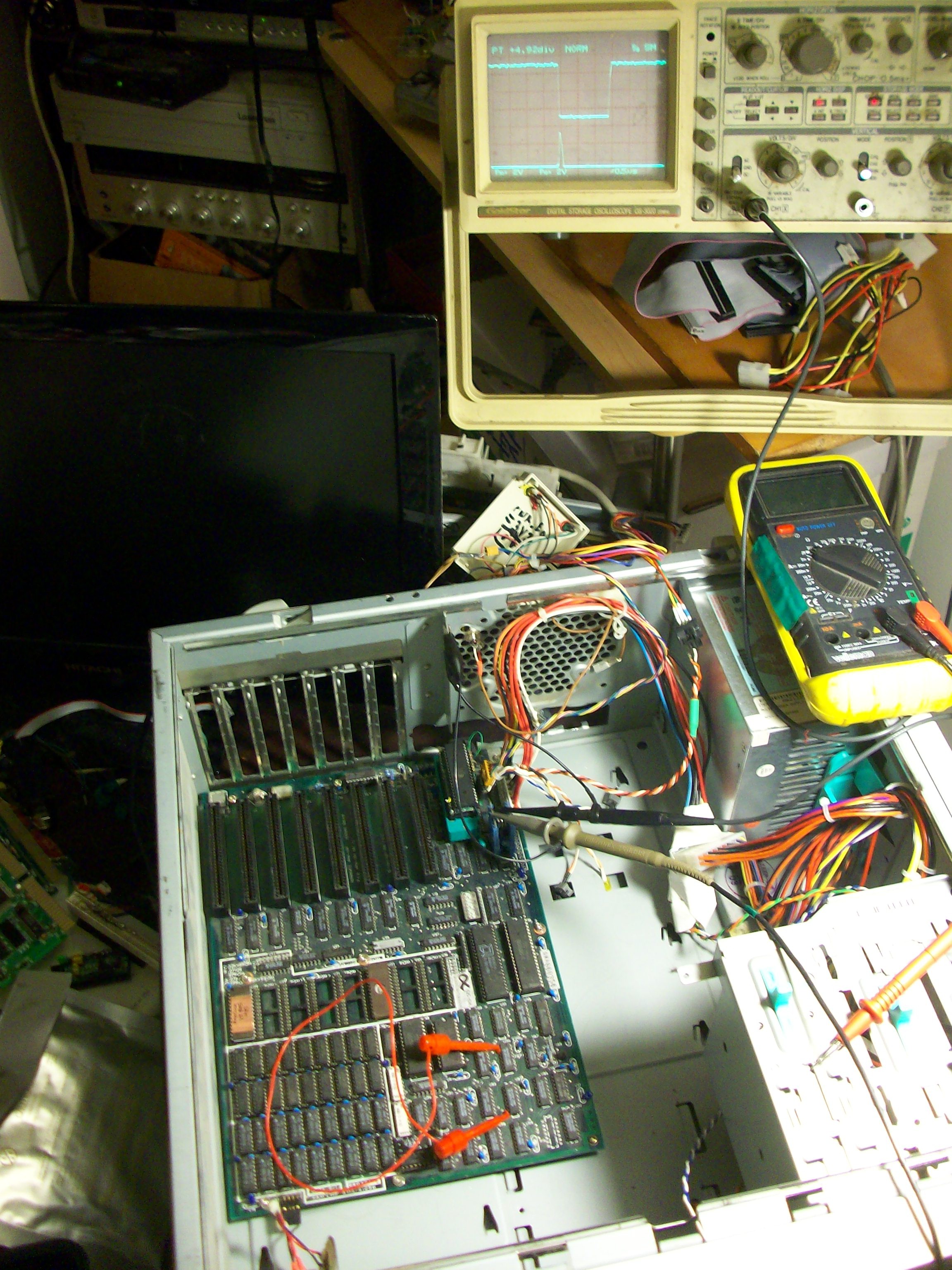
The ROM on the far-left is the BIOS (actually a copy, because I didn't want to risk damage to the original). The second ROM chip is actually the "Extension ROM" I made earlier.
AVR in a breakout-board mounted in a ZIF socket with combined ISP header and UART output dangling to the right. 'Scope shows /S1 which is driven low during a read-memory request by the AVR (or 8088) (top trace). The bottom trace shows the ALE output from the 8288. Note that ALE is <=1 bus-clock, so you can clearly see that the bus-transaction is taking *way* more than the allotted 4 cycles. (Artificial wait-states inserted by the AVR, and working!)
It's hard to see the clock-inverter/delay jumper, but it's the green wire behind the ISP header. Currently it's set to the output of the first inverter (I determined it should probably be connected to the output of the fifth, but I moved it around in earlier tests and forgot to move it back. Regardless, it's working! So, maybe all that worrying about meeting specific timings was a bit over-done... Par for the course.Also interestingly, the READY processing code works! I was afraid it wouldn't, because it takes several AVR instructions to read a pin, compare it, then jump, and all of that is supposed to happen in a single clock-cycle. But it works!
Looks like we're *right at* the limit of this analog/digital 'scope's digital abilities... It looks like I'm getting about 4-5 samples during each clock-cycle... which would make sense, it's a "20MHz" 'scope, in analog-mode... Don't recall seeing specs for the number of samples/sec in digital mode, but it's old (1980's), and 20MS/s sounds reasonable. (One nice thing about this 'scope is the fact it can switch between the two modes... I've actually managed to troubleshoot serial data-streams upwards of 100Mb/s in analog-mode).
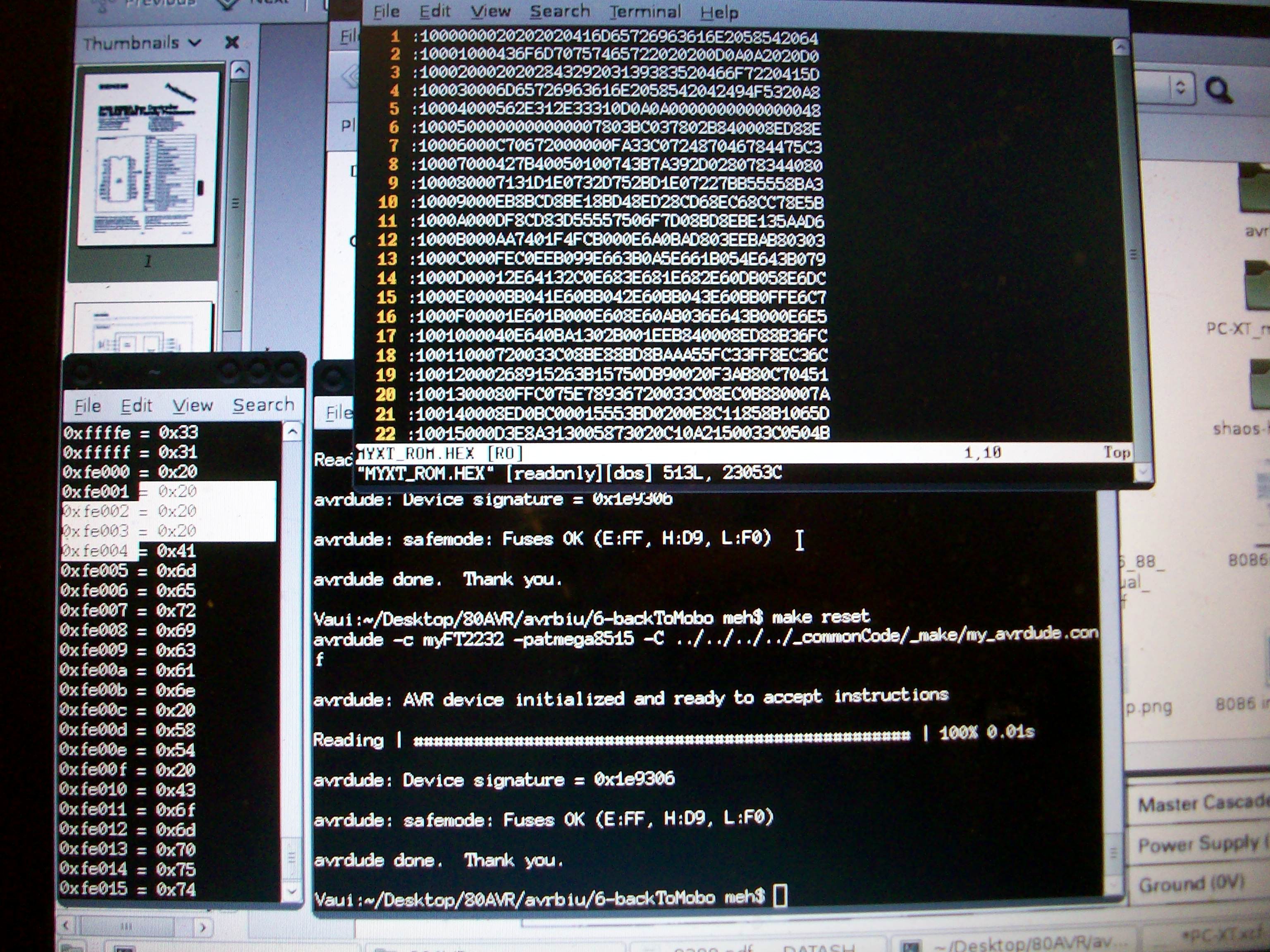
Here we have the serial-output on the left, showing the address and the read-back value. And that compares to the intel-hex dump of my ROM, which I did a while-back in my [E]EPROM programmer.
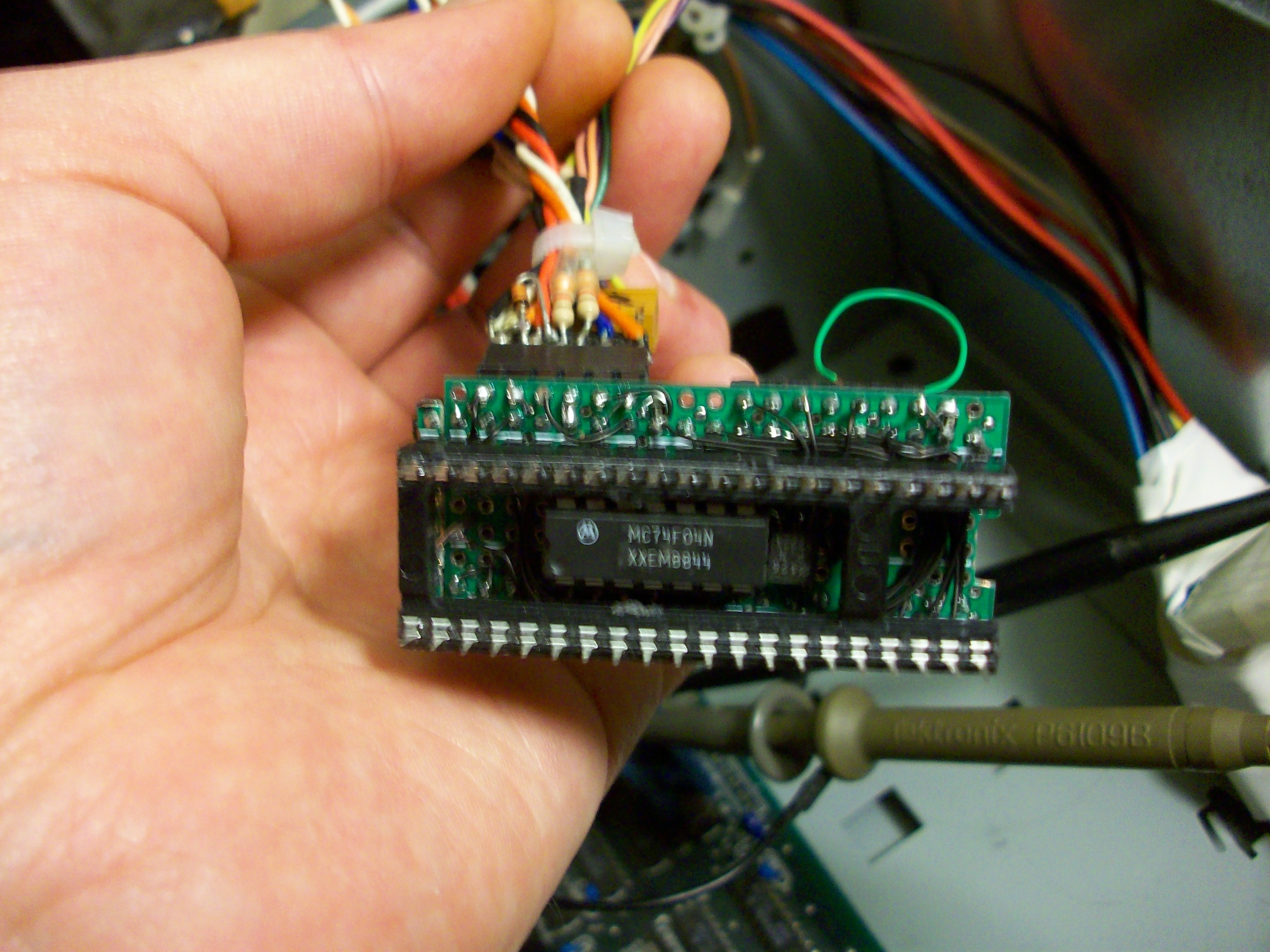
The 74F04 inverts the clock-signal, because the AVR works on rising-edge clocks, while the 8088's bus-interface expects the changes near (actually, slightly after) the falling-edges. The inverters are daisy-chained so I can select differing amounts of delays.
You can also see the 2N2222, used to invert the 8088's active-high RESET signal for the AVR's active-low, AND to isolate the In-System-Programmer's reset signal from the rest of the PC/XT motherboard.
The ISP header is wired-up at the top. All those resistors, wires, and diodes are part of my ISP dongle, allowing for a debug LED, a debug pushbutton, a reset button, and UART I/O all multiplexed on the ISP's header pins.
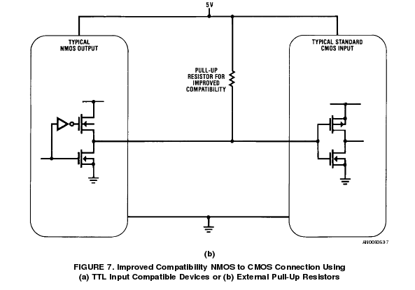
The green wire is currently jumpered to select the first inverter for the clock-signal. The network-resistor pulls up the A/D pins, which when driven by the bus (during "Read" requests) are driven by a TTL-LS, whose VOH-min is lower than the AVR's VIH-min. Apparently it's not uncommon to use pull-up resistors to interface TTL outputs to CMOS inputs... I found it in a app-note, and wrote about it in a previous log.
Here's an interesting thing:
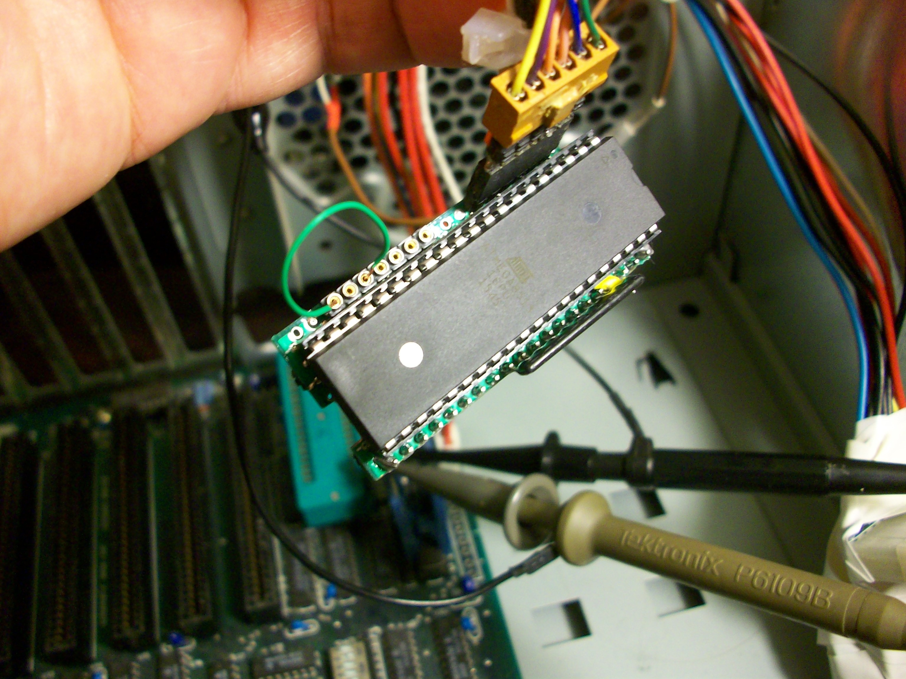
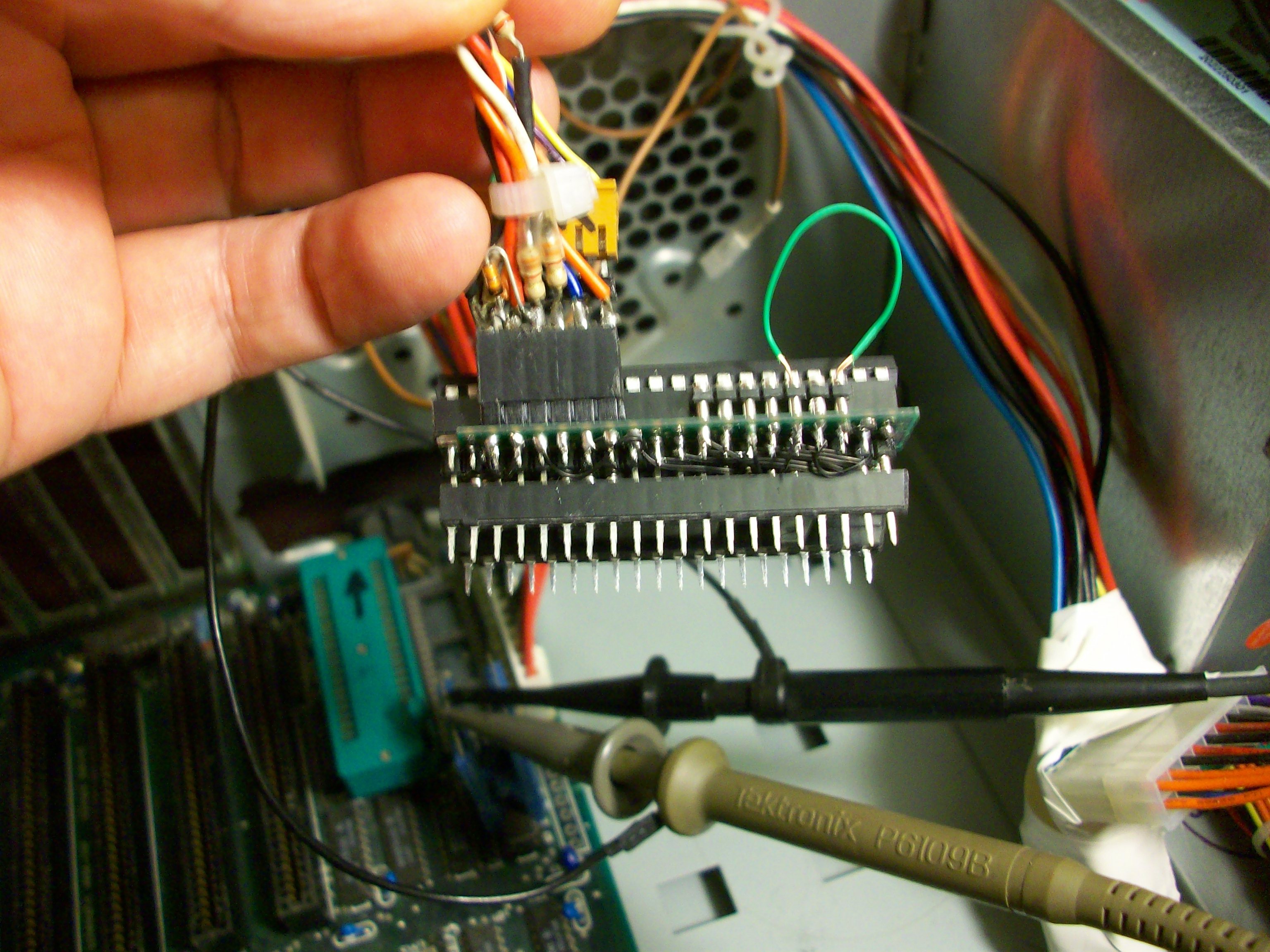
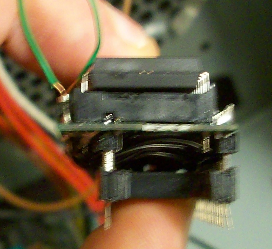
Shitty picture, but gets the point across... The sockets I used have a notch under them which I imagine is for exactly the purpose used, here... A row of pins can be soldered under it and protrude through the board, without interfering with the socket. Handy!
I used regular ol' header-pins for the 8088 pinout, then squished those into another socket whose pins are thinner and more like IC pins, to more-easily insert into sockets. (Squishing the header-pins into that socket required a lot of force, using a vice). I've done this once before, for this project, actually... when I made the ROM replacement for the SCSI card. Gotta make due with what I've got available!
You might've also noticed... I actually wire-wrapped to the header-pins (before crimping the socket onto it). That way the majority of the wiring could all be on the same side of the board... and gave me a reason to use my wire-wrapper, besides its handy stripper which I use all the time. So, they're wire-wrapped to the 8088's pinout, but soldered to the ATmega8515's socket. This also gave me some flexibility to run wires between header-pins.
But... there are a few pins (not currently implemented) which would be quite difficult to solder to, now that the whole thing's assembled. Ah well. I'm sure I can figure something out, should the time come.
-------------
Here's the code, extensive comments removed:
uint8_t bus88_read(uint8_t s20, uint32_t address) { uint8_t data; //### Bus is idle (assumed) ### //So, it should be OK to prep our Address bytes ADDR1916_PORT = (uint8_t)(address>>16); ADDR158_PORT = (uint8_t)(address>>8); ADDRDATA70_PORT = (uint8_t)(address); //Begin the Bus transaction S20_PORT = s20; // OUTPUT, AROUND: ¯|_ // The 8288 will bring ALE High... // ¯|_ ### T1 ### // The 8288 will bring ALE Low in 4-15ns after _|¯ //Nothing to do?! // Gotta keep the timing aligned... asm("nop;"); // ¯|_ ### T2 ### ADDRDATA70_DDR = ALL_INS; // >10ns AFTER ¯|_ // ¯|_ ### T3 / Tw ### while(!(READY_PIN & READY_MASK)) {}; //INPUT: <30ns AFTER _|¯ data = ADDRDATA70_PIN; //NOTE That we'll be in a later Tw, at this point... weeee! //Indicate that we're done with wait-states, and ready to enter T4 //8088: TCLSH Status Inactive Delay: after ¯|_ 10-130ns S20_PORT = S20_BUS_IDLE; //OUTPUT: >10ns AFTER ¯|_ // ¯|_ ### T4 ### // The 8288 will bring /IOR, /IOW, etc. high within 10-35ns of ¯|_ //Nothing to do?! asm("nop;"); // ¯|_ ### BUS IDLE ### // WARNING: This is NOT compatible with DMA and 8087! ADDRDATA70_DDR = ALL_OUTS; // >10ns AFTER ¯|_ return data; } -
x86 instruction-handling
02/03/2017 at 09:17 • 0 commentsI want to preface this with:
I do *NOT* Plan to emulate the x86 instruction-set for this project. It's not the goal. BUT the thought has been running through my head since the start, and I've gotten a bit carried-away with it a few times.
@Mark Sherman's #Cat-644 has a great explanation of how to speed-up instruction-emulation for instruction-sets where there's only one byte per instruction. That's a little bit difficult to apply to the x86 instruction-set because many (most?) instructions are multiple bytes. Though, n many cases those additional bytes are somewhat consistent, indicating the operands (and where/if to get them).
So, in addition to processing *instructions*, there's also processing of *operands*.
I've a vague idea of using this same scheme for those operand-bytes, essentially treating them *as* instructions.
The thing that makes this a bit weird is the fact that the instruction is grabbed *before* the operands. So, in the case of Cat-644, or FORTH, or whatnot, the idea is to load the operands into registers (or the stack) in early instructions, then the following instruction is *what to do* with them. In the case of the x86 architecture, however, it's the opposite... This is the instruction, now go get the operands.
So, my idea is somewhere along the lines of queuing the requested instruction, then loading the operands into registers, as though they were "mov register, operand" instructions, then, finally, to execute the queued instruction on those registers.
I think this could effectively reduce the number of *actual* instructions that need to be emulated, as well. E.G. There's 'add' which can be applied to two registers, or two memory locations, or a register and a memory location, and so-on. In one case there's a single-byte instruction used to indicate adding between two registers. In another case the instruction could be as many as 6 bytes (memory-to-memory, requiring addresses). Oh, and there's add 8-bit vs. add 16-bit, to boot!
Instead, implement *one* add instruction, add register to register. Always 16 bits.
But, since we don't know *what* to add, we first have to look at the first instruction-byte to determine the format of the opcode. If it requests additional bytes, then we queue the 'add', then process the second byte as though it consists of 'mov' instructions... 'mov tempOutRegister, memory', 'mov tempInRegister, register'. Then, execute 'add tempOutRegister, tempInRegister', and finally 'mov memory, tempOutRegister'.
I suppose, then, that last pseudo-instruction could, essentially, be another queued-instruction.
In a sense, intermediate instructions themselves are being pushed/popped.
It's still a bit vague, but I think it makes sense, and would probably be faster (and smaller) than having to jump to a function to grab instructions' operands, then return.
------
As far as 8-bit vs 16-bit...
Since the AVR is 8-bit anyhow, this is a bit easier than having to add tests and masks... Each emulated 16-bit register consists of *two* 8-bit AVR registers, already. So, one idea is to perform the 16-bit operation on two registers, then just optionally don't-copy back the high byte. Another idea is to essentially have a "scratch" register. E.G. in the case of "add8 registerOut, registerIn" which is implemented as a jump to "add16 registerOut, registerIn", registerOut consists of two AVR registers in both cases. But the high-register could, essentially, be like /dev/NULL. There'd be a real register that will actually take the high byte of the result, but that register will never be *read*. (Similar to how there's often a dedicated register storing the value '0'... usually this register is a real one which *can* store *any* value, but it's usually not used that way).
I'm not sure how relevant this is, any longer... It made sense in my early experiments, but I also did a lot with pointers, e.g. assigning registerOutH via pointer to the "null register". Pointers can be pretty expensive (and is there such thing as a pointer to a register in AVR's instruction-set anyhow? RAM sure...). It would probably make more sense to just use the same two registers for ins and outs, and move those values to the proper registers thereafter (as described earlier, using 'queued instructions').
-
Don't Trust Schematics!
02/03/2017 at 07:45 • 0 comments![]()
![]()
-----------
I'll come back to that.
First things first: Make sure you actually *call* your "init" function... Otherwise, yahknow, ports may not be initialized. And then you might see some interesting effects like "I know I'm writing 0 to that pin, why doesn't the 'scope trigger on it?!"
--------
Alright, now the 'scope shows it. Excellent.
Next step: Check that the 8288's responding to my AVR's control signals...
Checking the 8288's ALE output I see: Yep, there's a nice pulse coming out of the 8288's ALE. Excellent! Somewhere in my understanding of the 8088's bus-timings, I think I got *something* right!
Checking the 8288's /MRDC output I see... It's constantly high.
My ramblings from the other day led me to the conclusion that there's a case (especially when DMA is used) where the 8088 and the 8288 work together, regardless of the fact that the bus might be in use by other devices (such as DMA). The address-latching is definitely a part of that.
*IF* I can trust the schematic, (and, again, I'm working with a *clone* motherboard, not the IBM original that the schematic is supposed to relate to) the result is that when a DMA is in progress, the 8088 can still perform the vast-majority of a bus-transaction, but will be stalled by the READY signal's being unasserted. That means that the 8288's ALE must be strobed, to latch the 8088's requested-address, because the address-request happens *before* the READY signal affects the bus-transaction (by inserting wait-states).
So far, this is all looking pretty good.
In other ramblings from the other day I also came to the conclusion that I've left a few control-signals floating, which could feed back into the system causing trouble... The DMA controller, for instance, might be allowed to take control (even though it's not initialized). Or, judging by the slew of glue-logic that controls such things, it's entirely plausible the 8088 outputs I didn't implement (which are floating) might make it *look* like the DMA's doing its thing.
OK then.
Some questions: If the schematic matches, and If I understand the schematic correctly, I shouldn't be getting READY, ever. In which case, my software should be stalling, waiting for the memory device to become ready. It's not stalling, it's reading back 0xff.
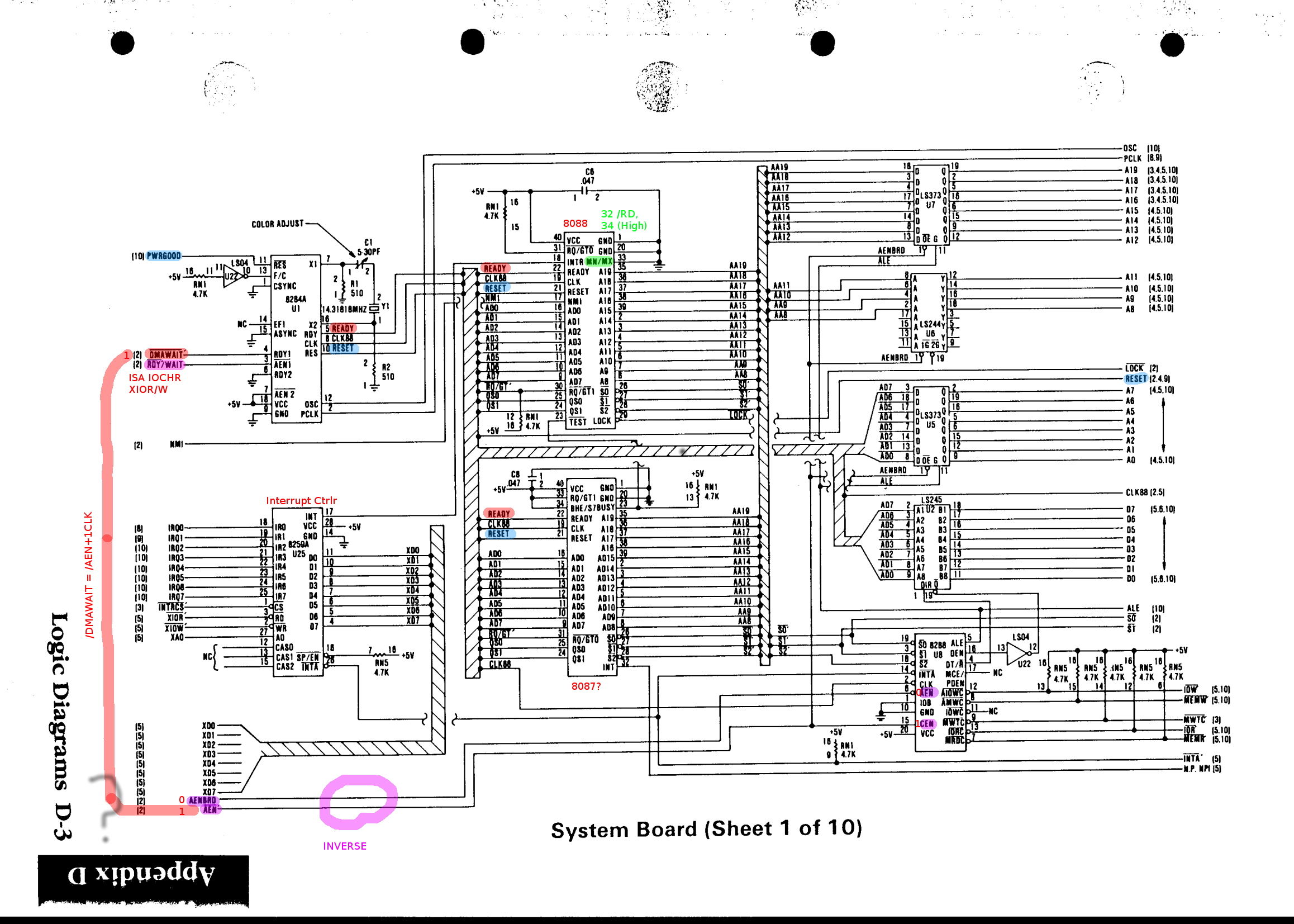
But, more interesting is the fact that the 8288's ALE happens but /MRDC doesn't... Because... I've checked the /AEN and CEN inputs... and both are low. So, address-enable is active, but command-enable is not active. That makes sense from the descriptions of these pins in the 8288 datasheet. But it DOES NOT match the PC/XT schematics, which clearly shows that /AEN is the Q output of a flip-flop, while CEN is the /Q output from the same flip-flop (and the 74LS175 doesn't allow for Q == /Q, unlike the 74LS74, where both Q and /Q can be high at the same time).
So... I think we've run into the first confirmed difference between the IBM PC/XT motherboard schematic and the clone motherboard I'm working with!
-------
The ramblings from the other day, again, listed several 8088-outputs I've not implemented. It was a bit ridiculous to think I could just leave them floating. I'll solder-up some pull-resistors next.
-
potential points of failure, and rambling about schematics
02/01/2017 at 21:44 • 0 commentsUPDATE 2-3-16: Adding fan-out info from the schematic (which isn't to be trusted)
UPDATE 2: and measurements from multimeter, + experiment with pulling down /LOCK.
-----------
Thoughts on possible 8088 outputs which are currently unimplemented that might help if they were...
Currently unwired (floating) 8088 outputs:
/LOCK - Pulling this low would likely assure that no other devices try to access the bus... (They shouldn't, since they haven't been initialized to do-so, but this shouldn't hurt). When active, devices shouldn't request to use the bus. Doing this would be a bit of a hack-usage of the signal but should be within-specs of the devices connected. Also, I don't see it's being pulled by resistors in the schematic, so currently it's floating. WHOOPS. Regardless, whatever it floats to, it shouldn't be paid-attention-to at this point, since, again, nothing that uses it has been initialized. But, floating-inputs have strange effects, sometimes...
[/LOCK Schematic Fanout = 1 LSTTL load, no pull-resistors. Pull-Down of LSTTL needs something like 330ohms!]
{Measuring diode-drop to V+... Yep... Floating input? Tied to ground with 100-ohm resistor, no change.}
/RQ / /GT1 - Pulling this high should do the same as /LOCK... (Note that both RQ/GT signals are pulled-high in the schematic, and /RQ / /GT0 is otherwise unwired). Any device requesting to use the bus would be denied. NOTE that since this is a bidirectional signal, and since the active-level is the same in each direction, the pull-up resistor needs to be small-enough to overcome *any* capacitance on the line *before* the next clock-cycle. Hmmm... (Would think that'd be inherent to the system design, but should probably look into this. Probably wouldn't hurt to pull it higher).
[/RQ / /GTn Schematic Fanout: RQ/GT0 = 0, pulled up via 4.7K; RQ/GT1 = 1 HMOS (8087), pulled up via 4.7K... Pull-Up, if not already, 10K should be OK]
{BOTH measure 4.7K to V+}
QS1:0 - Pulling these low should prevent any devices which use them (isn't that only the 8087, which isn't wired?) from ever trying to take over the bus... by tricking those devices into thinking every read-operation from the "8088" (AVR) is actually a memory or I/O read rather than an instruction-read which they might need to process. These guys aren't pulled-up in the schematic, but also looks like they're only wired to the 8087, which isn't installed.
[QS1:0 Schematic Fanout = 1 HMOS (8087), no pull-resistors. Fanout to HMOS, 10K pull-down should be OK, if there's a stray LSTTL not in the schematic we'd need more like 330ohms!]
{Not measuring anything between here and V+/GND. (8087 not installed). Maybe otherwise N/C.}
OTHERS:
Pin 34 - This pin is allegedly "always high" (output)... It shouldn't be wired anywhere, and is not shown on the schematic. But this motherboard is a clone, so who knows.
[Pin34 Schematic Fanout = 0, Allegedly N/C]
{Not measuring anything between here and V+/GND. Maybe N/C.}
/RD - The 8088, even in "maximum mode" (where it uses the 8288 to generate the /RD and /WR signals, as is the case in a PC/XT) outputs the /RD signal to one of its pins (why?!). The schematic shows it as N/C (logically). But, again, this is a clone, so I'd better verify that.
[/RD Schematic Fanout = 0, Allegedly N/C. If this is used on this mobo, then what???]
{Not measuring anything between here and V+/GND. Maybe N/C.}
/S2:0 = 0b100 - This indicates "Code Access" TODO: What makes that different from a Read-Memory (0b101)? Do the 8288's outputs respond differently, or does this go along with /QS1:0 to deviceswhich use them...(like the 8087)? Presumed: Code-Access only works on the memory-bus, anyhow (as opposed to I/O), and only as Read, and memory-devices (ROM/RAM) shouldn't care whether it's code or data, as far as how they respond...
Schematic-wise: /S2 is only wired to the 8088, 8087, and 8288... so shouldn't matter, for now.
/S1:0 is the same, but is also wired to a 4-input AND gate. 00, 01, 10 should have the same effect, regardless; forcing the output of the AND gate low, regardless of the other inputs. (Which seems strange, because its other inputs include the DMA-request, which would only be allowed when 11, which could occur during *both* "passive" (idle) mode, or "halt." Huh.) This same AND gate is also driven by /LOCK, so as long as that's low, that should do the same, here, as assuring that /S1:0 is never 0b11.[/S2:0 Schematic Fanout = 2 HMOS (8087, 8288) + 1 LSTTL (/S1:0). Not particularly relevant, since these are driven by the AVR.]
Also interestingly, the DMA request/grant scheme looks to rely only on whether the 8088/8087's bus units are idle (or halted), rather than the DMA controller's actually requesting a hold from the 8088. Which, looks like it's glue-logic implemented to have a 2-cycle delay guaranteed response of acknowledge, regardless of what's happening at that time (e.g. the bus was idle two cycles ago, but what if it's not NOW?). Not wrapping my head around how that'd *ever* work, considering the only time the bus would be idle (unless explicitly requested) is when the BIU's instruction-queue is full and no memory accesses are occurring (which seems quite seldom, considering the KIPS math I did earlier suggesting that the 8088's limited number of KIPS has more to do with the bus-bottleneck than its actual instruction-execution speed). Weird.
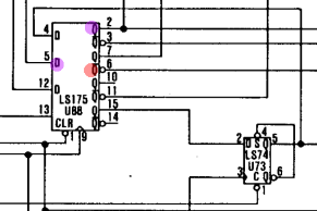
Here's a snippet:
![]()
The clear input to the LS74 is driven by HRQ_DMA, from the DMA controller, the Q output goes to HOLDA (at the DMA controller). As I recall, Clear and Set on a '74 affect the outputs regardless of the clock-input. If HRQ_DMA is high, and /LOCK and /S1:0 are also high, then pin13 on the LS175 is high. Oh, The LS74's Clear input is active-LOW, so cleared when the DMA controller is *not* requesting a hold. When *not* requesting a hold, the /Q output is high, which causes the Q output to be low, and thus HOLDA is inactive. OK.
When a hold-request is placed, regardless of the 8088's usage of the bus, the clear input goes high, but Q (and thus HOLDA) is still low, from before, and /Q is high. OK. Assuming the HRQ_DMA pin *stays* high AND the processor doesn't start a new transaction* (and/or finishes one)... (for at least one more clock cycle) the D-input will become high, the Q output (and thus, HOLDA) will follow on the next clock-edge (which is actually inverted on the LS74). The /Q output will then go low on that same clock-edge, which causes a "Set", the Q output will be forced to remain high, regardless of what happens on the D input. OK. (Wait, what? What if the CPU starts a new access?)
The HOLDA output (Q) feeds into the DMA controller, acknowledging the hold-request. Maybe then, or maybe later (after the DMA transaction?) the HRQ_DMA pin goes low, which pulls the LS74's CLEAR input active. Here's where it gets iffy. The LS74 has a strange state: When BOTH Set AND Clear are active (which they would be, here), BOTH outputs go high. OK. Q was already high. A high on /Q causes Set to be deactivated, but Clear is still active, causing Q to go low. OK. And as long as HRQ_DMA remains low (inactive) the HOLDA pin ignores D, remaining low... OK.
*Now, what happens if the processor starts a new transaction after HOLDA...? (And it looks like it could, for at least a couple clock-pulses thereafter!) The D input goes low. And we're assuming HRQ_DMA remains high, so the LS74's Clear input is inactive. Then D->Q. But No. Because Q was high, which means /Q was low, which means SET is active, which means the D input is ignored, which means the 8088's transaction will be ignored, which means the DMA transaction will still continue. SO, HOLDA (OR HRQ_DMA, as I would've assumed) must somehow be fed back to the CPU to prevent it from starting a new transaction.
But the only path back to the CPU appears to be via the READY/WAIT input... which doesn't *prevent* a transaction from starting, but causes an already-started transaction to wait for a while before completing. WHICH MEANS the 8088 will drive the address-bits at the same time as the DMA controller.
EXCEPT. There's another path from HOLDA that feeds into the 8288 controller. This disables commands and disables the address-latching... AND, all the 8088's address-bits are latched onto the address-bus via the 8288. OK.
INTERESTING.
So, if I understand this correctly... the 8088's READY input, in this case, tells the processor's bus-transaction, which has *already started* to WAIT.
But wait-states are only inserted AFTER T3.
And T3 is AFTER the processor has performed *several* transaction-functions... Including writing the address-bits, and latching them, and turning the address/data port into inputs for reading-back data, or writing the data bits to the port... It looks like the ALE output of the 8288 still functions, causing the CPU's address-latches to latch properly, but the output-enables aren't yet driven (by the same feedback path, from the HOLDA signal that stalls the 8288). OK... so the 8088 has *started* a transaction, (in fact, the majority of the transaction has already occurred) but the transaction is held via (indefinite) wait-states. The 8288 still *sees* the transaction, and follows-along in whatever internal state-machine it may have, but many of its outputs are disabled. So, it still follows-along with the 8088's transaction until it stalls.
(Bummer, I thought for a second, there, this arrangement might've been confirmation that the 8088 could interact with the 8288 more similarly to how I'm attempting with the AVR... e.g. setting up the address signals *way* before starting a transaction, etc.)
OK then. Interesting result 2: The READY signal *can* be stalled indefinitely (at least as long as the longest DMA burst!). That definitely seems to be confirmation that inserting "artificial" wait-states from the AVR's slow processing-time, should function. WHEW!
No... EXCEPT that, the 8288's Command Enable input is indirectly driven by the same source that deactivates the READY signal... so... IF it is a state-machine driven by clock-edges *until* T3, whereafter it masks the clock-signals by the CEN signal, there's no path for the processor to insert wait-states. IF it's NOT that sort of state-machine, but one wherein it acts on clock-edges *until* T3, whereafter its clock-signals are masked by the processor's /S2:0 outputs' not going "IDLE", then it should handle wait-states inserted by the CPU. (this is the case I presumed). HMMM...
I haven't seen anything to that level of detail in the datasheet.
That said, It also looks like the only two sources of READY's being deactivated are from IOCHRDY (from the ISA bus, which I'm not using) and the DMA controller (which I'm not using), SO, I should be able to get away, in this early stage, *without* the processor's reading the READY signal, at all, when accessing normal memory-locations (RAM or ROM) and just "dead-reconning" the number of bus-cycles. In which case, the system should've worked already, as-implemented, with a couple NOPs here and there, as long as my timings are correct.
Interesting result 3: The DMA controller can't be interrupted by the processor?!
Interesting... that might explain why e.g. the entire computer seems to stall when accessing floppy drives, etc. Surely they improved this in later systems, e.g. those that can run WinXP... Or do they just rely on the idea that most everything that needs to run (at least the mouse interrupts, etc.) is cached...? Weird.
See the problem...? I don't... That circuit's way too friggin' loopy.
-
firstGoNogo...
02/01/2017 at 14:00 • 8 commentsThe circuit from the last log is now wired-up, installed on the motherboard, and being tested with various programming...
Nogo, so far.
First, I tried to do it "blindly" with just an LED to indicate if data written to the DRAM on the motherboard was read-back incorrectly. The LED lit immediately on power-up.
After all that studying of the bus, I was pretty certain that'd've worked. So I fought with it for a while before resorting to a more reliable debugging-method.
On the plus-side, the pull-up resistor TTL->CMOS level-conversion seems to be doing the job, at least for the clock-signal (which has amongst the most strict input-level requirements).
I didn't have a 74S04, but I did have a 74F04, with similarly-spec'd propagation-delays. I installed a jumper-system so I could drive the AVR's clock from the inverter-chain after either one, three, or five inverters. (From timing-diagrams, I estimated that I need an inverted clock, and a slight delay, on the AVR's clock).
I was worried the AVR wouldn't like the 8088's clock, which is 4.77MHz, but with a 33% duty-cycle. But it doesn't seem to be complaining about that.
For Reset, I originally planned to use the sixth inverter, but it turns out my Schottky diode supply is quite limited (as in almost non-existent). The AVR's Reset signal is active-low, while the system's is active-high. Also I need to isolate the AVR's reset from the system reset, in order to use the in-system-programmer. To be within the AVR's VIL-max specs, a regular ol' diode (with a drop of about 0.65V) driven by a TTL chip with a VOL-max of >0.45V wouldn't do. I didn't even bother soldering that up. Instead, I followed a suggestion from a comment in the last log, and used a 2N2222 NPN resistor and a pull-up. I haven't tested that, as it looks like, from the schematics, the only source of system-reset is upon power-up... and the AVR's definitely running.
(Kinda ironic the PC/XT's active-high reset signal is controlled apparently-exclusively by the "Power-Good" signal. The point of Power-Good is to keep the system in reset until the power-supply has stabilized at ~5V. But, if the power-supply is "not good" at, say, 3V, then the output of the Reset signal couldn't be any higher than 3V, and technically that's not high enough for the active-high 8088's Reset Input's VIH-min. Of course, that VIH-min is assuming the chip is powered by 5V, and I'm sure they designed it to function.... but, an active *low* reset input makes a heck of a lot more sense to me.)
Since I'm not getting write-read tests to the DRAM to verify, I decided I needed to see what I was reading-back... I followed some other advice 'round here and opted to make use of the AVR's peripherals/software, rather than relying entirely on the system's peripherals... (I wouldn't be able to use the RS-232 ISA card to output data, if I can't write data to the ISA bus!).
So loaded up my usual AVR test-software, which includes a bitbanged serial-port on the ISP header. (I use bit-banged rather than the USART peripheral, because it can make use of the ISP header pins, rather than some random pin on another port that, in this case, is used for the Address Bus).
The result? Read-back from every address-location I've tried results in 0xff. I even tried reading data from the BIOS ROM, with the same results.
I've done a bit of "finagling" with the 8088's bus-timings to make this system possible... Including adding a *significantly long* and "artificial" "wait-state" when reading the actual system-READY signal (which requests wait-states). Removing the READY test and inserting various numbers of NOPs, instead, gives the same result. EXCEPT, when I use only one NOP (which, I think, should meet the bus-timing when no wait-states are requested, which *should* be the typical case). In that case, I read-back the low address-byte... (The low address-byte and the data-byte are multiplexed on the same port). So, at the very least, it would seem that the AVR is reading back the port correctly.
(Note that the AVR's inputs are delayed through a latch-system, so it may, in fact, be reading back the actual address written to the port, rather than, say, reading a floating-bus being slowly pulled up through resistors).
(Oh hey! Reading-back 0xff indicates that the pull-up resistors on the address/data port are doing their job!)
-----------
Anyways, not getting *anything* back from the ROM is plausibly indicative of something other than a problem with wait-states. (AS I UNDERSTAND: The READY signal *should* be active only when the device is actually ready to output data. And the output data *should* be held until the /RD signal is deactivated. And the /RD signal should only be deactivated after the CPU indicates it's done with the bus transaction... So if I insert some extra wait-states, via NOPs or via the delays caused by reading the READY signal, testing it, then branching, the data-output should still be valid until the /RD signal deactivates, which shouldn't happen until after I've read the data and indicated that the wait-states are complete.
Oy, long explanation to say, I think [mis]communication with the 8288 bus-controller might have something to do with this not functioning... The 8288 generates the actual /RD signal. And, the fact I'm not getting any data back (except the address written to the address/data port in the one case) suggests that the 8288's not generating a /RD signal.
And alllllll that to say... I should probably dig out the oscilloscope, and probably should look more into the schematics, as well.
So I should probably move this off my coffee table, before my apartment turns into the "to' up" mess it did last time... with 'scope on the couch, cat sleeping under the TV, and me sleeping upright on the remaining couch-space. Which means I should probably do some dishes... and some other cleaning. Klotski, much?
--------
Oh, and... There's this recurring *feeling* that maybe I'm just not initializing the system properly... But, remember, (as I understand from the schematics) the system-reset is controlled exclusively by power-up. Or, at the very least is *not* controlled by the 8088. The 8088 *has to* get *every* instruction from the bus, *immediately* after power-up-reset. Thus, immediately after power-up reset, the system *must* be initialized-properly to allow the CPU to access the ROM (DMA controller can't be interfering with bus transactions, due to not being properly-initialized, etc).
So, maybe, considering the only source of resets *after* power-up-reset is software-based (and thus controlled by the CPU, which must get its instructions *to* reset *from* the bus), there's no chance that, e.g. a software-reset could occur in the middle of a DMA transaction (or other device *using* the bus)... So, what I'm getting at is that there's a *slight* possibility that the AVR's exclusive reset-input (e.g. driven by the ISP) could allow it to reset at *any* time, rather than in response to a bus-read (of an instruction). So, it's *plausible* that the bus could be in an unknown state during an AVR-reset. OTOH, so far I haven't configured any other devices to use the bus, and, again, those devices *must* be power-up-initialized to *not* use the bus, so it should be that every device remains in their power-up-initialized state... And, again, whatever that state is, it must be conducive to the 8088's being able to immediately retrieve its first instruction from the ROM... Thus, I shouldn't have to initialize anything, nor cause a system-reset whenever I reset the AVR... right?
I certainly shouldn't have to respond to interrupts, nor even the Non-Maskable-Interrupt before interrupt-handlers have been loaded from the bus. ...
Hmm, I did leave some control-pins floating... Request/Grant...? This one's bidirectional. Hmmm... (nope, schematic shows it pulled-up on the motherboard).
Heh, don't trust the schematic:
Those are output-enable inputs, the top chip didn't fit in the screenshot is a 74LS244. None of those signals are outputs. What's driving 'em?![]()
The bottom chip drives the "NMI Enable" signal...
Yep, need to grab the 'scope.
And not only don't trust the schematics because there's obviously an error (and maybe more)... but also because this is a *clone* motherboard, rather than an IBM original.
(heh, this was just going to be a couple lines saying essentially "it's soldered-up, programming, but doesn't yet work")
-
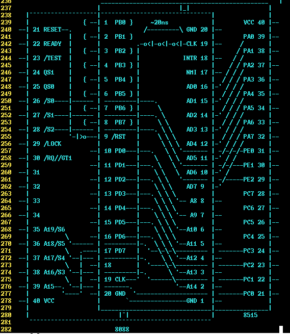
ATmega 8515 in an 8088 socket, pin-mappin
01/28/2017 at 19:56 • 5 comments![]()
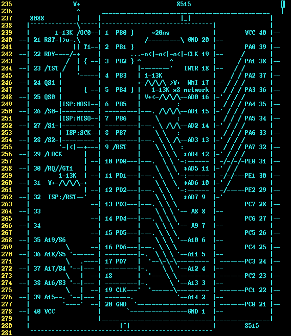
Originally I planned on flipping the 8515 upside-down. GPIO-wise that'd've aligned quite nicely. But most of the AVR peripherals I might use are on PORTB. Also, I want it socketed (maybe I'll replace it with an ATmega162 in the future, etc.). So, instead of flipping it upside-down, I've resorted to rotating it 180deg.
On the motherboard, there's little space at the "top" end of the 8088 (where pins 1 and 40 are located) because of the keyboard connector, otherwise it'd make a *shit-ton* of sense to shift the 8515 "down" (up in the pinout diagram) by three pins.
------
To meet "hold"-times on the bus, the clock-signal needs to be delayed between 10-30ns, because the AVR's outputs occur on the rising-edge of its system-clock. I'll probably use a 74S04 to create the delay. It specs roughly 4ns propagation-delay per inverter. (Wow, I didn't realize how fast the old-school BJT-series could get!) Five of those in series would give me 20ns. And, importantly, also invert the signal.
The 8515 documentation actually says that the internal system-clock isn't perfectly-aligned with the external clock input, and worse that [mis]alignment is device/temperature-dependent.. But, interestingly, it doesn't state that in the section regarding PORT/PIN timings, nor anywhere else I'd seen in 15years of using AVRs. I discovered it recently in the section regarding the External Memory Interface (which most AVRs don't have). (Interesting this information-tidbit never came up during #sdramThing4.5 "Logic Analyzer" or the versions prior, which rely heavily on synchronous operation with the clock-input. Though, this may explain some unexpected timing-differences I'd worked around.)
Thus, using 5 inverters at 4ns would give 20ns delay, which is perfectly inbetween the 10-30ns range. Should I find that doesn't work due to delays in the AVR's external/internal clocking system, I can also choose to tap after 1 or 3 inverters.
Using a 74S04 leaves one inverter for the reset signal... though I'm contemplating whether/how that'll work, since I plan to use In-System-Programming, which needs to drive the AVR's reset signal (and plausibly the entire system's).
--------
I haven't yet verified this, but I'm pretty certain the AVR's clock and reset inputs are compatible with TTL output-levels. Being that many crystal-oscillators have TTL-level outputs, and I'm pretty certain I read that the RESET pin has different thresholds than the GPIOs...
....AND NO. WTF.
AVR:
- Normal pins: VIL<=0.2*VCC, VIH >=0.6*VCC.
- VIL <= 1V
- VIH >= 3V
- RESET: VIL<=0.2*VCC, VIH>=0.9*VCC (!?)
- VIL <= 1V
- VIH >= 4.5V
- XTAL1: VIL<=0.1*VCC, VIH>=0.8*VCC (?!)
- VIL <= 0.5V
- VIH >= 4V
That doesn't even make sense... at 5V, that means XTAL1 has VIL <=0.5V! That's even *lower* than TTL! (Usually CMOS inputs have *higher* VIL-max). And 4.5V for VIH-min?! Heck, the AVR's *outputs* don't even guarantee these values!
OK, got some thinking to do again. Weee!
--------
As for the rest of the circuit... I need to look into the PC/XT schematic, again. My hunch (which, obviously has been wrong before), is that devices don't drive the 8088's data-inputs directly. Otherwise, here's the rationale: Some motherboards have 80C88's and are expected to work with the same ISA cards. *Adding* a buffer (HCT) in between, on these newer motherboards, would add delays which (if the original TTL/NMOS motherboard design *didn't* have a buffer) wouldn't be accounted-for in the timings specified by the original TTL/NMOS design. Thus, the additional delay would have to be accounted for with increasingly complex circuitry and/or wait-states. However, I did read somewhere that an 8088-based system can be upgraded to an 80C88 system by merely replacing the necessary TTL glue with HCT glue... so no extra delays accounted for. (OTOH, aren't HC components slower than LS?).
Now, that's *just* thinking about it from the *timing* perspective. The other perspective is in consideration of output-strength of the devices... There are a *lot* of devices on the bus... a large fanout. 8 ISA cards, the 8088, the DMA controller, timer, keyboard controller, and more. Seems to me, intuitively, they'd've broken that up a bit with buffers (in the original TTL/NMOS design).
Off to find out just how wrong I am...
Oh, so the thought is... assuming there's a 74x245 (TTL) buffer on the data-lines, I could probably swap it out with a 74HCT245, if necessary. Kinda destroys the
"drop-in-replacement" aspect of this project. But, adding a 245 on the AVR's "daughter-board" would be a bit difficult, since the direction-signals aren't driven by the CPU, but from the 8288. Oy.(And, I still need to look into the other signals, driven by other sources, e.g. the clock-driver handles the clock-output and the READY signal). This is losing its fun-quality fast.
![]()
----------
74S04:
- VOH-min@1mA >=2.7V (Nogo. Pull-ups?)
- VOL-max@20mA <= 0.5V (close enough? No way I'm drawing 20mA)
It's somewhat doubtful I have 74HCT's that can be used as inverters in-stock, and that they're as fast as the 74S series... I do have 74ACTs which are even faster, I think... maybe too fast, hmmm... And, not '04s, so I'll probably have to string together a bunch of NANDs.
/RD output!
The 8088, even when running in "Max-mode" (as it does on a PC motherboard) has a /RD output! This guy's unwired on the PC/XT motherboard, so I didn't include it in my pinout. But, if I implemented it in the AVR, it could handle swapping the direction of an "on-daughter-card" 74HCT245... Allowing for a CPU-drop-in-replacement as preferred, rather than having to modify the motherboard. (And, realistically, I could've implemented that even if the original 8088 didn't have a /RD output. Duh). Of course, this'll add a delay... is that a concern?
My current timing-scheme (in a recent log), which has been simplified *dramatically* from earlier expectations, relies somewhat heavily on the fact that only one AVR instruction must be executed during each bus-cycle. BUT, in an earlier (overthinking) log, I mentioned a way to change 9 pins in the same AVR instruction-cycle... The idea is to set up an AVR timer several cycles earlier, with an output pulse when you want it. The /RD pin would be a perfect use for this. (I feel like I read about this somewhere, but I was stupid and didn't bookmark it). At the bus cycle when the /RD pulse is emitted, we also have to change the port to inputs, using up the AVR's one-instruction-cycle during that bus cycle.
Data lines:
Looking at the schematic, yes, there is a 74LS245 between most devices and the CPU's data lines. The only exception I see is the 8087 which connects directly to the 8088. (I'm not yet implementing 8087 support, and maybe I have an 80C87, anyways?). I think I see this 'LS245 on the motherboard. Unfortunately, not socketed. Or, maybe fortunately since I wanted this AVR-thing to be drop-in...
SN74LS245 (onboard, driving 8088 data-inputs)
- VOL@12mA <= 0.4V (OK)
- VOH@3mA >= 2.4V (Too low. Can I use pull-ups?)
NEC uPD8088D (Same as HMOS-II Intel 8088 Specs):
- VIL <= 0.8V
- VIH >=2.0V (NOT RQ/GT pins! Where are they listed? Nor apparently the clock-inputs?)
- VOL@2mA <= 0.45V
- VOH@0.4mA >=2.4V (TTL-ish)
- VIL-CLOCK <= 0.6V
- VIH-CLOCK >= 3.9V (interesting, similarly different to other I/Os as the AVR's)
NEC uPD8284AD clock generator (CLK / READY -> 8088):
(CLOCK output, doesn't really matter since I've got to drive it through an inverter, anyhow. But READY is a concern).
- VOL<=0.45V
- VOH-CLOCK@1mA >=4.0V
- VOH-other@1mA >= 2.4V (e.g. READY, too low... pull-ups?)
-----------------
AVR inputs are rated for -0.5V to VCC+0.5V... could this be useful?
I'm not building a product, here... I just want to get programming!
So, let's say we ran the AVR off 4.5V, instead...
- Normal pins: VIL<=0.2*VCC, VIH >=0.6*VCC.
- VIL <= 0.9V (was 1V)
- VIH >= 2.7V (was 3V)
- RESET: VIL<=0.2*VCC, VIH>=0.9*VCC (!?)
- VIL <= 0.9V (was 1V)
- VIH >= 4.05V (was 4.5V)
- XTAL1: VIL<=0.1*VCC, VIH>=0.8*VCC (?!)
- VIL <= 0.45V (was 0.5V)
- VIH >= 3.6V (was 4V)
Specifications listed earlier for other chips are mins/maxs... NOT typicals. And, in many cases, ratings given for much greater loads than the AVR (and other circuitry) would impart.
Kinda ironic, The 74S04 happens to have VOH >= 2.7, which now meets our VIH... except it's not connected to a GPIO, but to the XTAL1 and RESET inputs, which it's not even close to meeting specs for. And the 74LS245 --which does drive the pins that are now capable of VIH >= 2.7V--(as well as the clock-generator which drives READY) only guarantees VOH >=2.4V.
Weee!
---------------
I guess, then, there's good reason I've been lagging on actually soldering this stupid thing up... Looks like I'll be needing more support-circuitry than I planned to make this even reliable enough to experiment with. weeee...
--------------
Pull-up resistors for TTL -> CMOS:
I knew I read it somewhere...
https://www.fairchildsemi.com/application-notes/AN/AN-314.pdf
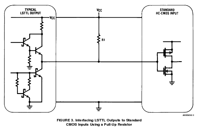
Since LSTTL specifications guarantee a 2.7V output high level instead of a 3.5V output high, when designing to the worst case characteristics greater compatibility is sometimes desired. One solution to increase compatibility is to raise the output high level on the TTL output by placing a pull-up resistor from the TTL output to VCC, as shown in Figure 3.
When the output pulls up, the resistor pulls the voltage very close to VCC. The value of the resistor should be chosen based on the LSTTL and CMOS fanout of the LS gate. Figure 2 shows the range of pull-up resistors values versus LS fanout that can be used. For example, if an LSTTL device is driving only CMOS circuits, the resistor value is chosen from the left axis which corresponds to a zero LSTTL fanout![]()
No mention of how *fast* this is... Nor why one wouldn't just choose this route rather than using HCT components. I'm sure other documents (probably ones I've read) go into that in more detail.![]()
I'm not too fond of adding more chips to this thing, so I'll use some rationalizing to justify why people might choose HCT over pull-ups *besides* the likely speed-increase (since 4.77MHz isn't *that* fast, right?).
My rationale for the use of HCTs over pull-resistors is that they can easily be dropped-in-place of other chips that already exist (like the 74LS245). But, since my '245 is soldered-in, and I don't want to modify the motherboard to make this work, that'd mean I'd have to add *another* HCT245 inbetween. So, whatever speed-increase may be gained by using a HCT245 *as* your receiving CMOS device (rather than adding pull-ups) won't be gained, here, because the HCT245 would be inserted *between* the sender and the receiver. So, it'd probably be faster, anyhow, in this case, to just use pull-up resistors. Whew. Network-resistors are easy.
No mention of how to *calculate* the VOH value you'll get when using a specific resistor-value... but my theory is that since the LS high-side driver is, essentially, an emitter-coupled voltage-follower, the pull-up resistor will, essentially, cause the high-side NPN to turn off (the pull-resistor's voltage would be higher than the base). That's my theory, and I'm sticking to it.
So, now... That leaves us with... If this is driving anything *other* than CMOS, there might be trouble, because the pull-resistor might act as a voltage-divider with whatever else is connected.
So, now... I need to make sure wherever I'm throwing these pull-resistors won't be connected to anything other than CMOS inputs.
---------
From there... There's another consideration. Some of our sources *aren't* TTL, despite having TTL-level outputs. The clock-driver appears to be NMOS or HMOS.Thankfully, that same document has a discussion about H/NMOS as well, and says that it can be treated similarly to TTL. Add Pull-Ups.
Actually, it says it's probably not necessary to add pull-ups, but can "improve compatibility."![]()
Which, realistically, is probably the same for TTL when very weakly-loaded (as will be the case in this circuit), and I could've probably just wired the danged thing up as I'd originally planned without messing with any of this.
--------
So, back to the schematic... Do I need to worry about voltage-dividers when using pull-ups?
The only CPU inputs being implemented, thus far, are AD7:0 (data inputs), CLOCK, and READY. CLOCK is connected to my 74S04, or whatever... So pull-ups are occurring *after* the 74S04. The only load is the AVR's CMOS inputs. OK. READY looks like it's only connected to the 8088 and 8087... 8087's Not Yet Installed (and is HMOS, anyways, which allegedly looks like CMOS, load-wise). So, no problem there. Now, DATA.
DATA, when reading (when we'll need to use the pull-ups) comes from the LS245, and fans-out to the 8088 and 8087, which should be fine. But ALSO routes to a 74LS343.
The '373 input *might* interact with that pull-up resistor to create a voltage-divider, in which case it kinda nullifies its purpose. Funny they didn't mention that in the .... wait... they did! Figure 2.OK, LSTTL-Fan-Out = 1. and CMOS-Fan-Out doesn't count. So, allegedly, I can get away with a pull-up resistor anywhere from 1-13Kohms. I'm pretty sure I've got some network-resistors in that range.
Nice. And this thing should work...
The only problems, then, should be my lack of understanding of the bus... software... right?
Now I want to get this blasted thing running. But beer sounds a lot better, even if it is alone on a Saturday Morning and will leave me literally flat-broke until... Wednesday(!?)
-------
But first... What was my beef with the 74S04 that might lead me down a different route...? Didn't I mention ACT NANDs or something...? Nothing, nothing we haven't already covered... Pull-Ups will fix it.
So, we should be at the point where I can solder this danged thing up and ...
Nope.
RESET and the In-System-Programmer.
The RESET input is one-way... The clock-generator chip is responsible for the RESET signal, and it's apparently not open-collector. So, the ISP's /RESET signal won't reset the rest of the system, and must be isolated from it.
OY.
On the plus-side, I've left PORTB un-mapped, so far... And that's where the ISP pins connect. So, for these early experiments, I don't have to worry about what the rest of the system is doing while the ISP is programming. WHEW. (Note to self, remove hard disk for these experiments!)
(NOTE 1-31-17: I've just checked, and the 8284 clock/reset/ready generator chip does *not* stop outputting the clock signal during reset. Otherwise there might've been some difficulty ISProgramming an AVR whose clock is externally-driven. OTOH, the ISP's reset signal will *not* feed back into the motherboard, so I guess it wouldn't matter anyhow. AND the reset signal apparently *only* happens during power-up, as it's only tied to the Power-Good signal. Interesting.)
So, I'll take the output from the 74S04 and feed it through a diode, thus making it essentially open-collector, active-low-only. OK.
This should do...
![]()
- Normal pins: VIL<=0.2*VCC, VIH >=0.6*VCC.
Improbable AVR -> 8088 substitution for PC/XT
Probability this can work: 98%, working well: 50% A LOT of work, and utterly ridiculous.
 Eric Hertz



 Shitty picture, but gets the point across... The sockets I used have a notch under them which I imagine is for exactly the purpose used, here... A row of pins can be soldered under it and protrude through the board, without interfering with the socket. Handy!

