0%
0%
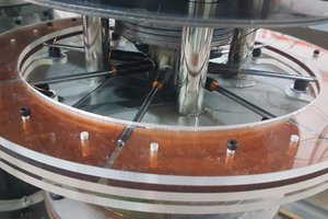
RFET - Resistance Field Effect Transistor
A new transistor type, the RFET requires no semiconductor material and is 3D printable. It is my creation shared with you.
 Les Hall
Become a Hackaday.io member
Already have an account? Log in.
Just one more thing
To make the experience fit your profile, pick a username and tell us what interests you.
Pick an awesome username
hackaday.io/
Your profile's URL: hackaday.io/username. Max 25 alphanumeric characters.
Pick a few interests
Projects that share your interests
People that share your interests


 Agustin Cruz
 Joshua R. Taylor
 Anderson Antunes
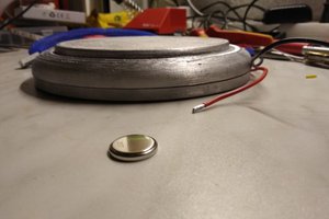
Thanks for your interest. I'm open to team collaborations. Les