 Nguyen Vincent
The second iteration of the board aims to correct all of the mistakes that were spotted when testing the first iteration:
- Selection of a very low quiescent current LDO. This LDO also has a shutoff pin, which can be controlled by the MCU. This is very useful for example to disconnect power-hungry peripherals when the board is idle.
- Better clearance for cables. One of the cables in the first iteration could not be plugged without cutting some of the flaps. In the new iteration, I took care to keep proper clearance between the cable housing and other components.
- Fixed some of the hardware issues, like missing traces or misplaced connections, improper length tuning, ...
- Use of tented vias. This made soldering a bit easier especially close to the MCU.
- Compatible with both memory displays and e-paper displays.
For this iteration, I used ENIG finish, which provides excellent planarity.
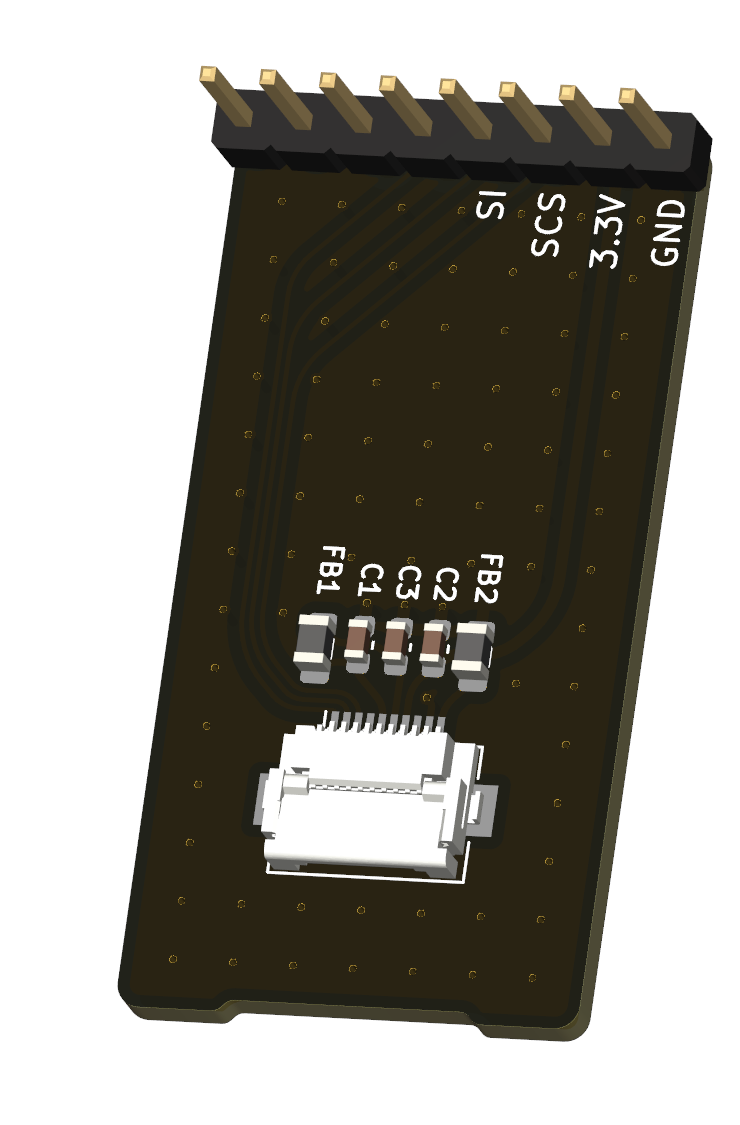
As I mentioned in an older log, the e-paper display was quite noisy when exposed to direct light (and even worse with sunlight, which, for a solar-powered board, is obviously not ideal). I then chose to design a breakout for the LS011b7dh03 from Sharp Devices. This breakout is mechanically compatible with the previously designed e-paper display, with an almost identical footprint.
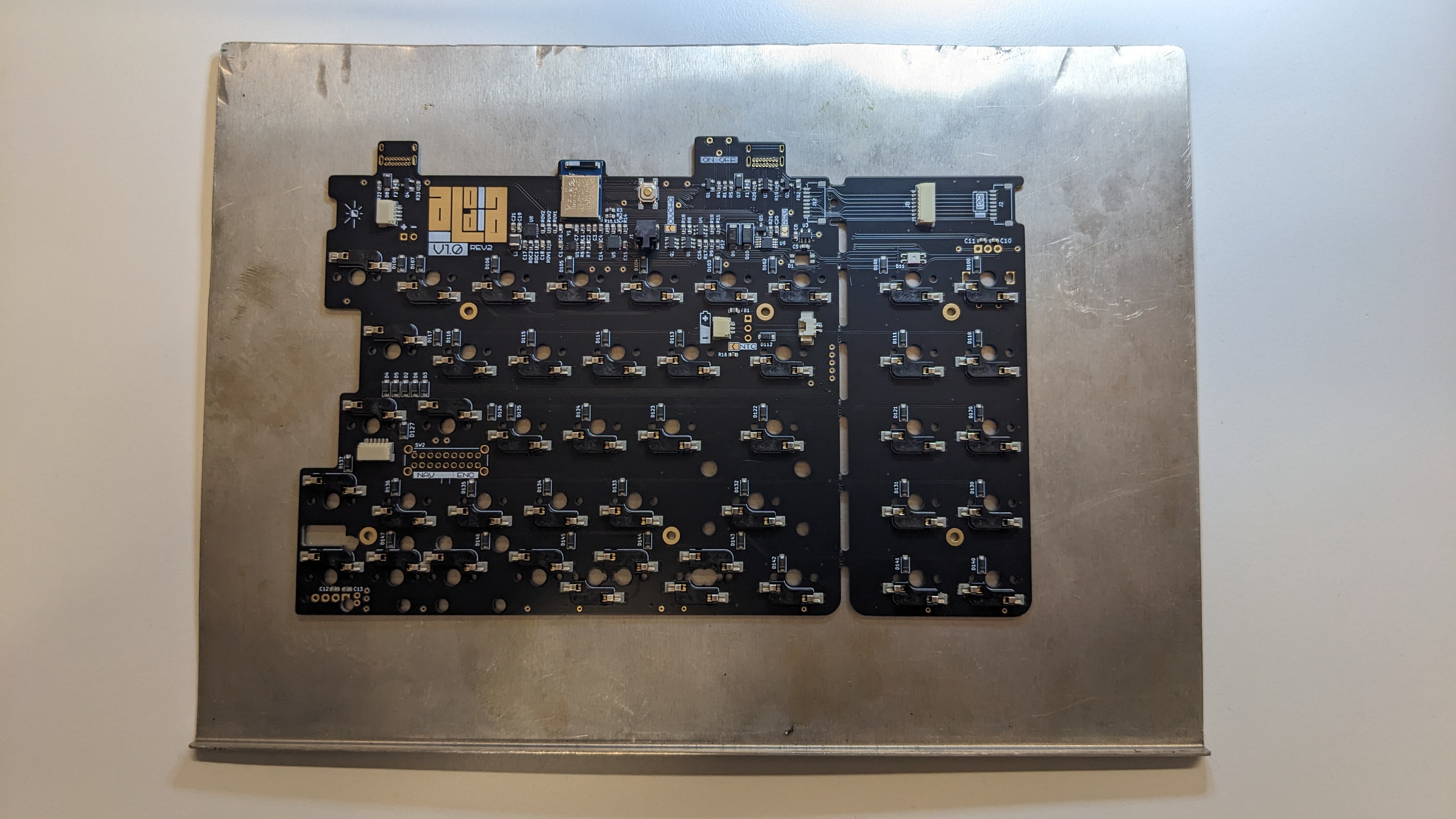
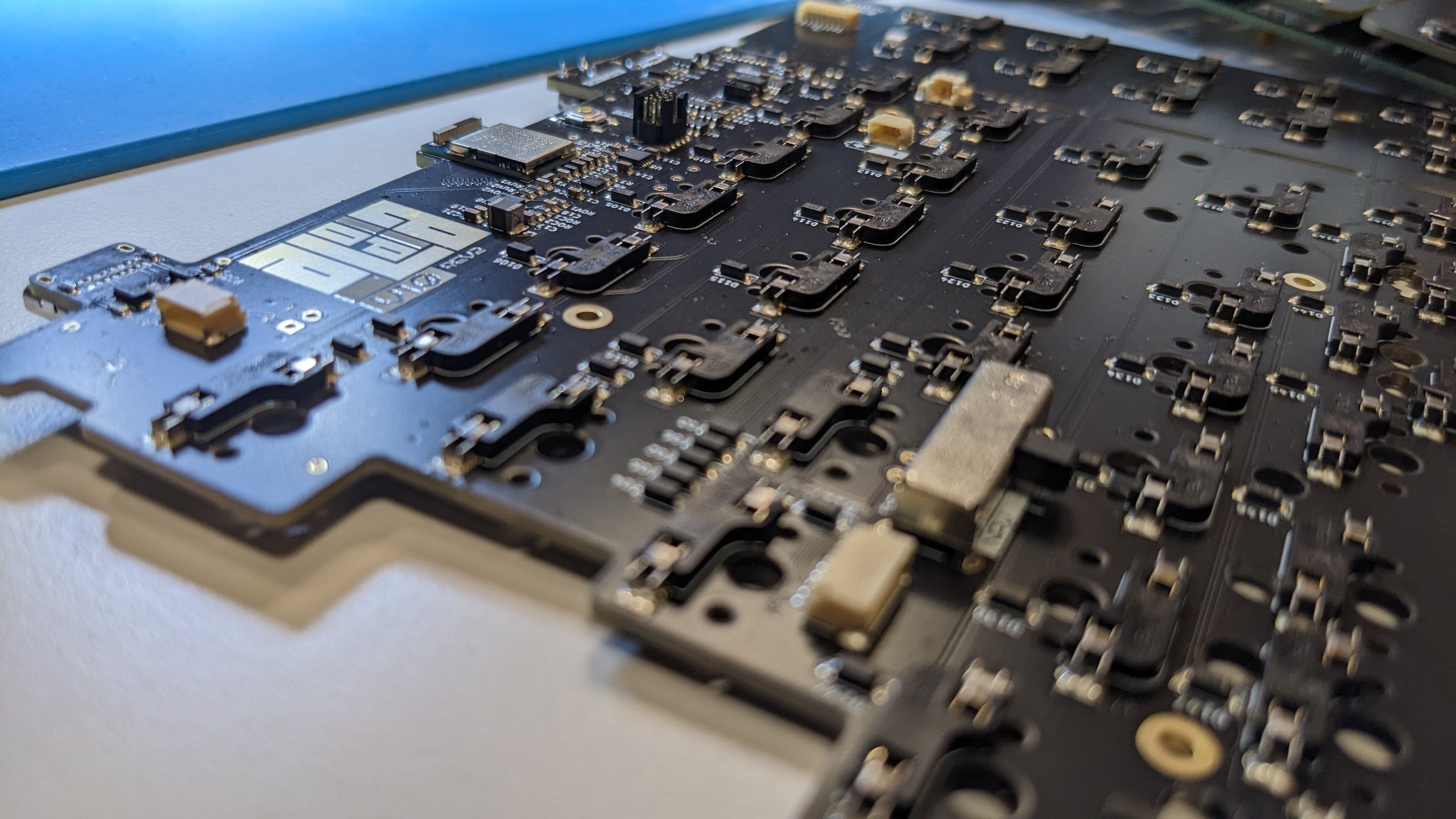
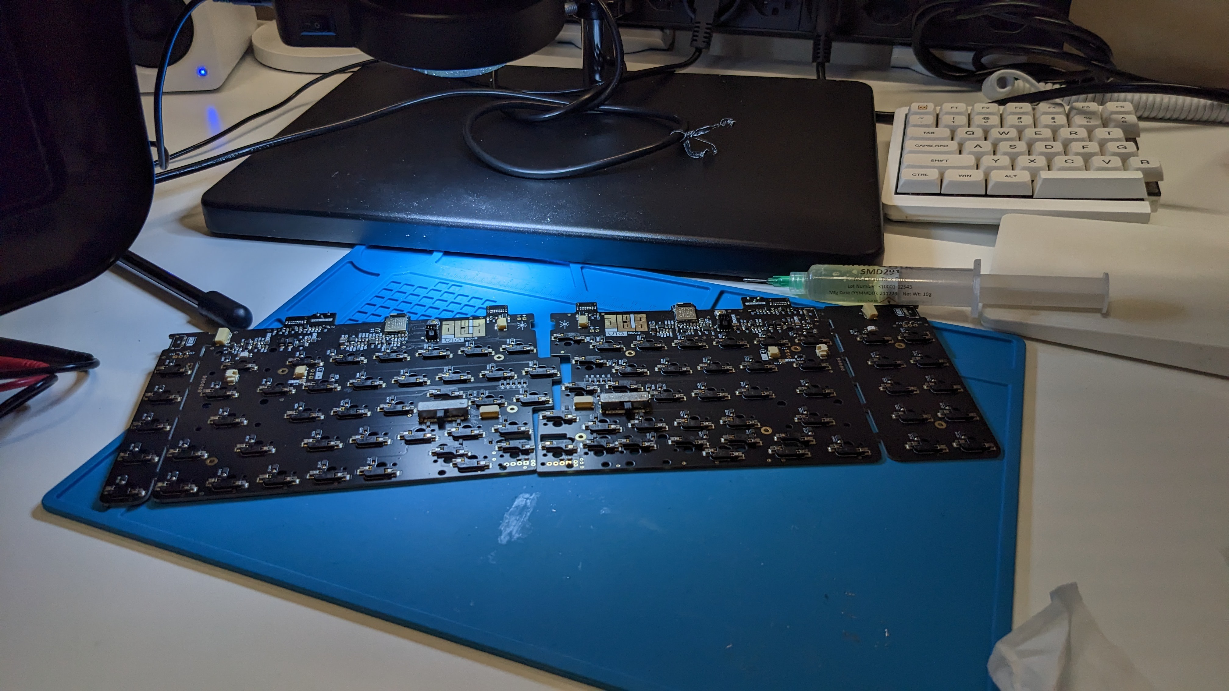
Assembling the boards
Aloidia rev2 PCB assembly - YouTube
Left half fresh out of the oven
After soldering the THT components:
The two halves assembled:
Discussions
Become a Hackaday.io Member
Create an account to leave a comment. Already have an account? Log In.